
Reference voltage driver

A reference voltage and driver technology, applied in the direction of electrical components, logic circuits, logic circuit connection/interface layout, etc., can solve the problems of reducing the output level of the amplifier and the large offset voltage of the transistor

Pending Publication Date: 2020-10-27
SEMICON MFG INT (SHANGHAI) CORP +1
View PDF0 Cites 0 Cited by
  • Summary
  • Abstract
  • Description
  • Claims
  • Application Information

AI Technical Summary

Problems solved by technology

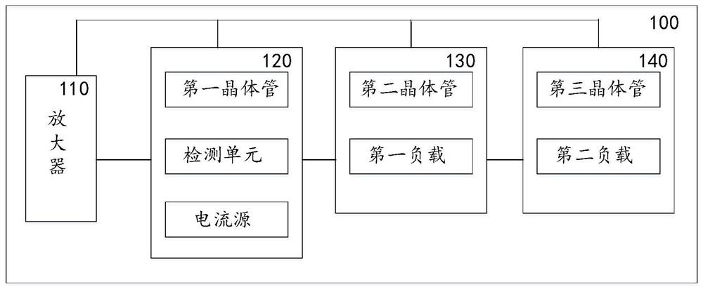
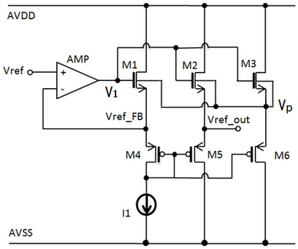
[0004] The purpose of the present invention is to provide a reference voltage driver, the transistors in the master and slave output stages share a well region, which solves the problem of large offset voltage of the transistors and does not increase the parasitic capacitance of the transistors in the master and slave output stages; The reference voltage driver has no padding effect that reduces the output level of the amplifier

Method used


Image

  • Reference voltage driver
  • Reference voltage driver

Examples


Embodiment Construction

[0022] As mentioned in the background, traditional reference voltage drivers used in analog-to-digital converters usually use an amplifier and a master-slave output stage structure, which has the problems of large transistor offset voltage and large parasitic capacitance in the master-slave output stage, and the amplifier’s The problem is that the output level is large.

[0023] The inventors found that there are usually three connection methods for the substrates of the transistors in the master and slave output stage structures. The first type: both are connected to the power supply; the second type: both are grounded; the third type: each is connected to an independent well. The substrates of the transistors in the master and slave output stage structures are respectively connected to independent wells, and the transistors in the master and slave output stage structures have relatively large offset voltage and increased parasitic capacitance. The substrates of the transist...


PUM


Abstract

The invention provides a reference voltage driver. The reference voltage driver is characterized in that the driver comprises an amplifier, and a main output stage, a slave output stage and a well bias unit which are respectively connected with the amplifier; the main output stage comprises a first transistor, the slave output stage comprises a second transistor, and the well bias unit comprises athird transistor; the three transistors share one well region, and the well is connected with the source of the third transistor; the source voltage of the second transistor is equal to the source voltage of the first transistor, the source voltage of the second transistor is an output reference voltage, and the source of the third transistor generates a well bias voltage equal to the output reference voltage. The first transistor and the second transistor share one well region, so that the matching degree is increased, the problem of relatively high offset voltage is solved, and parasitic capacitance is not increased. And the source voltage and the substrate voltage of each transistor in the three transistors are equal to each other and are at the same level, so that the substrate bias effect is eliminated, and the output level of the amplifier is reduced.

Description

technical field [0001] The invention relates to the technical field of semiconductor integrated circuits, in particular to a reference voltage driver. Background technique [0002] Analog-to-digital converters (ADCs) are widely used in circuits, and normally the normal operation of the analog-to-digital converters (ADCs) requires a reference voltage driver to provide a stable reference voltage. The accuracy, stability and noise performance of the reference voltage driver directly affect the performance of the ADC. [0003] Traditional reference voltage drivers used in analog-to-digital converters usually use an amplifier and a master and slave output stage structure. There are large transistor offset voltages in the master and slave output stages, increased parasitic capacitance, and a larger output level of the amplifier. question. Contents of the invention [0004] The purpose of the present invention is to provide a reference voltage driver, the transistors in the mas...

Claims


Application Information

Patent Timeline
IPC IPC(8): H03K19/003H03K19/0185
CPCH03K19/00384H03K19/018507
Inventor 陈廷乾
Owner SEMICON MFG INT (SHANGHAI) CORP
Learn More