Power semiconductor device and manufacturing method thereof

A technology of power semiconductors and manufacturing methods, which is applied in the direction of semiconductor devices, semiconductor/solid-state device manufacturing, electrical components, etc., and can solve problems such as open circuit status of devices, failure at the terminal of the chip table top, etc.

Active Publication Date: 2020-11-13
ZHUZHOU CRRC TIMES SEMICON CO LTD
View PDF5 Cites 0 Cited by
  • Summary
  • Abstract
  • Description
  • Claims
  • Application Information

AI Technical Summary

Problems solved by technology

[0003] In view of this, the embodiment of the present invention provides a power semiconductor device and its manufacturing method, which solves the problem that the current standard GCT chip structure is prone to failure at the end of the chip mesa in the overvoltage blocking state, causing the device to fail in an open state The problem

Method used


Image

  • Power semiconductor device and manufacturing method thereof
  • Power semiconductor device and manufacturing method thereof
  • Power semiconductor device and manufacturing method thereof

Examples


Embodiment Construction

[0026] The following will clearly and completely describe the technical solutions in the embodiments of the present invention with reference to the accompanying drawings in the embodiments of the present invention. Obviously, the described embodiments are only some of the embodiments of the present invention, not all of them. Based on the embodiments of the present invention, all other embodiments obtained by persons of ordinary skill in the art without creative efforts fall within the protection scope of the present invention.

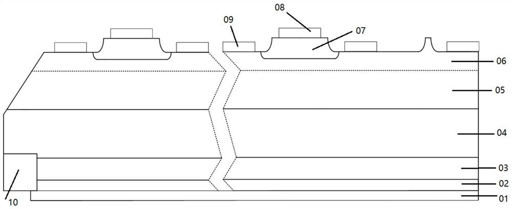
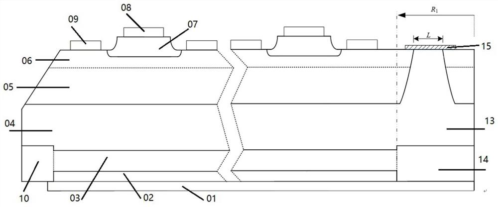
[0027] The power semiconductor device described in the present invention may be a GCT. Such as figure 1 As shown, the existing GCT mainly includes a PNPN four-layer structure vertically. According to the degree of doping, it can be subdivided into P+ transparent emitter anode 02, N' buffer layer, N - Base 04, P Base 05, P + Base 06 and N + Emitter 07 (also called cathode comb). In addition, GCT can also include anode 01, cathode 08, gate 09 and N...


PUM

PropertyMeasurementUnit
depthaaaaaaaaaa

Abstract

The invention provides a power semiconductor device and a manufacturing method thereof, and solves the problem that a standard GCT chip is easy to fail at a chip mesa terminal in an overvoltage blocking state, and further causes that the device fails and is in an open circuit state. The device comprises a functional region and a voltage breakdown region, the voltage breakdown region is close to the central position of the power semiconductor device, is surrounded by the functional region, and comprises a second conductive type short circuit structure and a convex second conductive type base region which are stacked in sequence, and the second conductive type short circuit structure penetrates through a first conductive type transparent emitting anode and a second conductive type buffer layer of the functional region; the convex second conductive type base region penetrates through a first conductive type first base region, a first conductive type second base region and a second conductive type region, and a protruding part is formed in the extending direction of the second conductive type base region towards the first conductive type base region.

Description

technical field [0001] The invention relates to the technical field of semiconductors, in particular to a power semiconductor device and a manufacturing method thereof. Background technique [0002] GCT (Gate Commutated Thyristors, Gate Commutated Thyristors), as a fully-controlled power semiconductor device, has great potential for future applications in flexible DC grids due to its large blocking capability, low on-state loss, and large power capacity. There are three PN junctions in the existing GCT device, and the junctions from the anode to the cathode are J 1 junction (anode transparent junction), J 2 junction (blocking voltage main junction) and J 3 junction (gate-cathode junction). GCT is divided into four working states: trigger (open), on-state, off and blocking. When the GCT chip is in the overvoltage blocking state, it is necessary to apply a reverse bias voltage within -20V (or short circuit) to the gate-cathode of the device to avoid a significant drop in t...

Claims


Application Information

Patent Timeline
Patent Type & Authority Applications(China)
IPC IPC(8): H01L29/06H01L29/744H01L29/74H01L21/332
CPCH01L29/0615H01L29/0684H01L29/744H01L29/7424H01L29/7436H01L29/66393
Inventor 陈芳林徐焕新陈勇民操国宏蒋谊潘学军邹平孙永伟
Owner ZHUZHOU CRRC TIMES SEMICON CO LTD
Why Eureka
Try Eureka