Avalanche photodetector and preparation method thereof

An avalanche photoelectric and detector technology, used in circuits, electrical components, semiconductor devices, etc., can solve the problems of uneven electric field distribution in the absorption area and unsatisfactory gain-bandwidth product.

Active Publication Date: 2020-11-13
WUHAN OPTICAL VALLEY INFORMATION OPTOELECTRONICS INNOVATION CENT CO LTD
View PDF4 Cites 6 Cited by
  • Summary
  • Abstract
  • Description
  • Claims
  • Application Information

AI Technical Summary

Problems solved by technology

[0003] However, the current avalanche photodetectors have disadvantages such as unsatisfactory gain-bandwid

Method used


Image

  • Avalanche photodetector and preparation method thereof
  • Avalanche photodetector and preparation method thereof
  • Avalanche photodetector and preparation method thereof

Examples


preparation example Construction

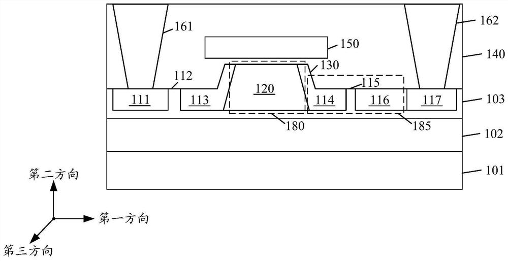
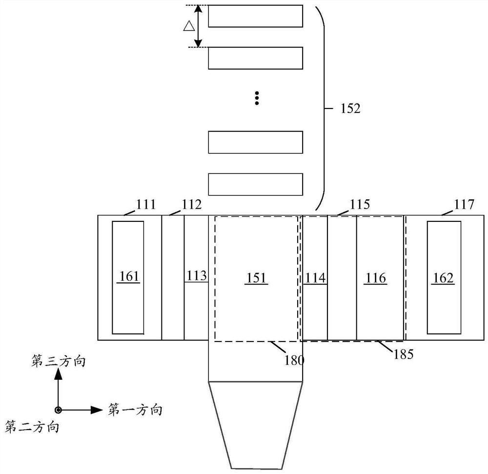
[0118] The embodiment of the present invention also provides a preparation method of avalanche photodetector with lateral structure; for details, please refer to the attached image 3 . As shown, the method includes the following steps:

[0119] Step 201, providing a substrate, the substrate including a first semiconductor material region;

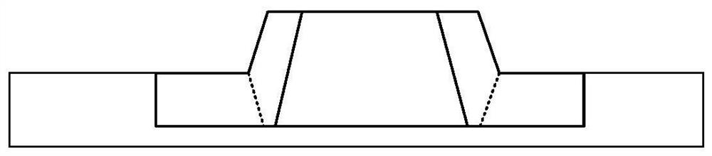
[0120] Step 202, performing an etching process on the first semiconductor material region to form a groove deep inside the first semiconductor material region;

[0121] Step 203, performing a selective epitaxial growth process to form a first epitaxial growth layer in the groove, the material of the first epitaxial growth layer being a second semiconductor material different from the first semiconductor material;

[0122] The first epitaxial growth layer is formed as an absorption region of the avalanche photodetector; the upper surface of the first epitaxial growth layer is a light absorption surface, and the light absorption surface pr...


PUM


Abstract

The embodiment of the invention discloses a lateral structure avalanche photodetector and a preparation method thereof. The lateral structure avalanche photodetector comprises a substrate, a first epitaxial growth layer and a second epitaxial growth layer, wherein the substrate comprises a first semiconductor material region; an avalanche region is formed in the first semiconductor material region; the first epitaxial growth layer is formed as an absorption region; the upper surface of the first epitaxial growth layer is a light absorption surface and protrudes out of the upper surface of thefirst semiconductor material region; the lower surface of the first epitaxial growth layer is lower than the upper surface of the first semiconductor material region; the second epitaxial growth layerat least comprises a first part and a second part which are located on the two sides of the first epitaxial growth layer in the first direction, the first part and the second part cover two side walls, which protrude out of the first semiconductor material region, of the first epitaxial growth layer respectively, and the first part and the second part form at least one part of a first charge region and a second charge region respectively; and the first charge region, the absorption region, the second charge region, and the avalanche region at least partially overlap in the first direction.

Description

technical field [0001] The invention relates to the technical field of photon integrated chip detection, in particular to an avalanche photodetector and a preparation method thereof. Background technique [0002] Photodetectors are one of the key optoelectronic devices in optical communication, optical interconnection and optoelectronic integration technologies. They are widely used in various fields of military and national economy, and avalanche photodetectors are widely used for their high responsivity and sensitivity. The market welcomes. [0003] However, the current avalanche photodetectors have disadvantages such as unsatisfactory gain-bandwidth product and uneven electric field distribution in the absorption region, so further improvement is needed. Contents of the invention [0004] In view of this, the embodiments of the present invention provide an avalanche photodetector and a manufacturing method thereof to solve at least one problem existing in the backgroun...

Claims


Application Information

Patent Timeline
IPC IPC(8): H01L31/107H01L31/0232H01L31/0236H01L31/18
CPCH01L31/1075H01L31/02327H01L31/02363H01L31/1804Y02P70/50H01L31/105H01L31/035281H01L31/022408H01L31/028H01L31/107
Inventor 胡晓肖希陈代高王磊张宇光李淼峰
Owner WUHAN OPTICAL VALLEY INFORMATION OPTOELECTRONICS INNOVATION CENT CO LTD
Why Eureka
Try Eureka