Photoconductive switch with electrode pre-set solder and manufacturing method thereof

A photoconductive switch and electrode technology, applied in circuits, electrical components, semiconductor devices, etc., can solve problems such as charge concentration, and achieve the effect of improving the withstand voltage and reliability, and improving the reliability of electrode connection.

Active Publication Date: 2022-04-12
SHANGHAI SPACEFLIGHT ELECTRONICS & COMM EQUIP RES INST
View PDF5 Cites 0 Cited by
  • Summary
  • Abstract
  • Description
  • Claims
  • Application Information

AI Technical Summary

Problems solved by technology

[0004] The object of the present invention is to provide a photoconductive switch with electrode preset solder and its manufacturing method, which can effectively solve the problem of charge concentration caused by welding solder bumps on the electrode of the photoconductive switch; use the method of presetting solder on the electrode of the photoconductive switch to precisely control the solder Positioning and Solder Shape and Thickness

Method used


Image

  • Photoconductive switch with electrode pre-set solder and manufacturing method thereof
  • Photoconductive switch with electrode pre-set solder and manufacturing method thereof
  • Photoconductive switch with electrode pre-set solder and manufacturing method thereof

Examples


Embodiment 1

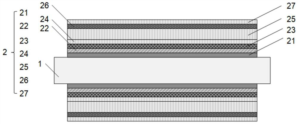
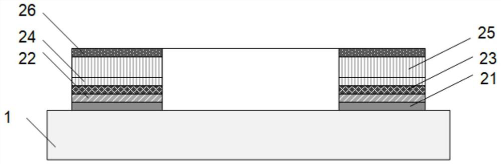
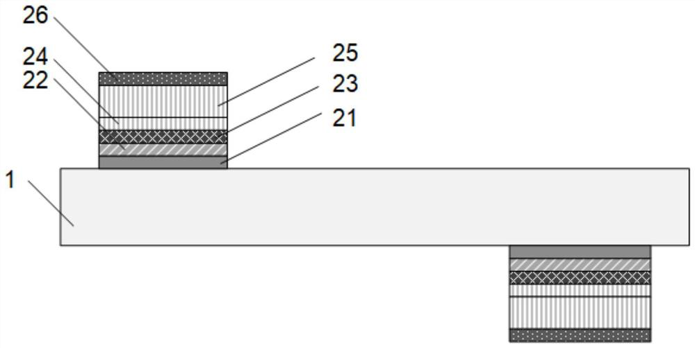
[0045] see figure 1 As shown, this embodiment provides a photoconductive switch with electrodes pre-prepared with solder, including a silicon carbide substrate 1 and two electrodes 2:

[0046] The silicon carbide substrate 1 includes opposite first surfaces and second surfaces. In this embodiment, the silicon carbide substrate 1 is a semiconductor silicon carbide wafer doped with carriers;

[0047] Two electrodes 2 are arranged on the first surface and / or the second surface of the silicon carbide substrate 1, and the electrodes 2 include a Ni layer 21, a TiW layer 22, a Pt layer 23, a first Au layer 24, and a second Au layer stacked in sequence. 25 and Sn layer 26, and the Ni layer 21 is located on the side close to the silicon carbide substrate 1, wherein the mass ratio of the second Au layer 25 to the Sn layer 26 is 8:2, so the second Au layer 25 and the Sn layer 26 are processed by heat treatment After forming Au80Sn20 to form a eutectic solder layer;

[0048] In this exa...

Embodiment 2

[0052] see Figure 4 to Figure 10 As shown, based on the same inventive concept, the present invention also provides a method for preparing a photoconductive switch with electrode preset solder, comprising the following steps:

[0053] S1: providing a silicon carbide wafer 1 and processing the silicon carbide wafer 1 to a required size;

[0054] S2: Processing mask tooling 3, see Figure 5 Image 6 , Figure 7 As shown, the mask tooling 3 includes a base 31 and a mask steel plate 32 stacked up and down. A number of chip placement grooves 311 consistent with the size and thickness of the silicon carbide wafer 1 are provided on the base 31. According to the shape of the electrode 2, the mask steel plate 32 An electrode groove 321 is provided at a position corresponding to the wafer placement groove 311;

[0055] In this embodiment, the base 31 and the mask steel plate 32 are square, and each of the four corners of the base 31 is provided with a base screw hole 312, and each ...

Embodiment 3

[0065] This embodiment is a specific application of Embodiment 2. This embodiment provides a method for preparing a photoconductive switch with electrodes pre-prepared with solder, and this embodiment takes the structure of electrodes facing opposite sides as an example to illustrate, including the following steps :

[0066] 1. Select a carrier-doped semiconductor silicon carbide wafer 1 and process it to the required size. In this embodiment, the silicon carbide wafer 1 is processed to 10mm×10mm×1mm. The side of the silicon carbide wafer 1 fed into the laser needs to be polished ;

[0067] 2. Process the mask tooling 3, first process the base 31, and cut out a wafer placement groove 311 of 10mm×10mm×1mm in size consistent with the wafer size and thickness on the base 31, and a plurality of wafer placement grooves 311 can be processed on the base 31, In this way, multiple wafers can be processed in the same batch, which is more efficient than photolithography; positioning pin...


PUM


Abstract

The invention discloses a photoconductive switch with electrodes pre-prepared with solder, which comprises a silicon carbide substrate and two electrodes, the two electrodes are arranged on the first surface and or the second surface of the silicon carbide substrate, and the electrodes include sequentially stacked Ni layer, TiW layer, Pt layer, first Au layer, second Au layer and Sn layer, and the Ni layer is located on the side close to the silicon carbide substrate, wherein the second Au layer and the Sn layer form a eutectic solder layer, the traditional solder There is poor placement accuracy in the sheet melting welding method. The solder sheet is thicker, and it is easy to form a bump after soldering, resulting in charge concentration. By presetting the solder film layer on the electrode, the positioning of the solder can be precisely controlled, and the thickness and shape of the solder can be effectively controlled. , improve the electrode connection reliability of the photoconductive switch, thereby improving the withstand voltage capability and reliability of the photoconductive switch.

Description

technical field [0001] The invention relates to the field of packaging of semiconductor devices, in particular to a photoconductive switch with electrodes pre-prepared with solder and a manufacturing method thereof. Background technique [0002] The photoconductive switch (PCSS) is a switch controlled by light. Because of its ps-level response speed, large power capacity, small size, and the use of optical pulse triggers without electromagnetic interference, it can generate high-power pulses, ultra- There are extremely wide applications in fields such as fast photoelectric control and terahertz sources. Compared with crystal materials such as Si and GaAs, SiC crystal material has the advantages of high breakdown field strength, large band gap, fast saturation electron velocity and high thermal conductivity, and is an ideal substrate material for photoconductive switches. [0003] In order to realize the potential of SiC materials in the field of high-temperature, high-frequ...

Claims


Application Information

Patent Timeline
Patent Type & Authority Patents(China)
IPC IPC(8): H01L31/0224H01L31/08H01L31/18
CPCH01L31/0224H01L31/08H01L31/1812Y02P70/50
Inventor 罗燕袁涛周义丁蕾林闽佳王立春姚崇斌
Owner SHANGHAI SPACEFLIGHT ELECTRONICS & COMM EQUIP RES INST
Why Eureka
Try Eureka