Wearable multi-size universal machining platform for chip

A processing platform and wearable technology, applied in electrical components, semiconductor/solid-state device manufacturing, circuits, etc., can solve the problems of difficult chip clamping and fixing, complex chip circuits, affecting chip processing, etc., to achieve convenient handheld operation and compact structure. , the effect of convenient operation

Pending Publication Date: 2020-12-01
东莞市中帆新材料科技有限公司
View PDF0 Cites 0 Cited by
  • Summary
  • Abstract
  • Description
  • Claims
  • Application Information

AI Technical Summary

Problems solved by technology

[0003] Chips are used in various industries. Because the chips are relatively small, it is not easy to clamp and fix the chips on the workbench when operating and processing the chips, which will affect the processing of the chips, and the chips are also susceptible to moisture. , during processing, if the processing is carried out in a humid environment, the internal circuit will be damaged and the chip will be damaged. Moreover, the circuit on the chip is more complicated and requires welding and other operations. The chip is relatively small and difficult to observe clearly. , Chips are mostly used in scientific and technological research and development laboratories, and are also used in mobile phones or smart industries. During the research and development process, chips need to be processed repeatedly. However, different chips need to be processed on different processing platforms. There will be different sizes. When processing chips of different sizes, different processing platforms need to be used for processing, which is very inconvenient. Therefore, it is urgent to develop a wearable multi-size general processing platform technology for chips.

Method used


Image

  • Wearable multi-size universal machining platform for chip
  • Wearable multi-size universal machining platform for chip
  • Wearable multi-size universal machining platform for chip

Examples


Embodiment Construction

[0027] The technical solutions in the embodiments of the present invention will be clearly and completely described below with reference to the accompanying drawings in the embodiments of the present invention. Obviously, the described embodiments are only a part of the embodiments of the present invention, but not all of the embodiments. Based on the embodiments of the present invention, all other embodiments obtained by those of ordinary skill in the art without creative efforts shall fall within the protection scope of the present invention.

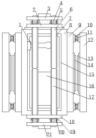
[0028] see Figure 1-5 , the present invention provides a kind of technical scheme:

[0029] A wearable multi-size universal processing platform for chips, comprising a mounting plate 8, side plates 9 are symmetrically bonded on the left and right sides of the mounting plate 8, and a gripping plate 12 is provided on the outside of the side plate 9, and the gripping plate 12 A second coil spring 10 is symmetrically connected with the ...


PUM


Abstract

The invention aims to solve the problem that a chip is not easy to process conveniently in the prior art. The invention discloses a wearable multi-size universal machining platform for a chip. The platform comprises a mounting plate. Side plates are symmetrically bonded to the left side and the right side of the mounting plate. Holding plates are arranged on the outer sides of the side plates. Second spiral springs are symmetrically connected between the holding plate and the side plate, guide rods are sleeved with the second spiral springs, a second contact piece is bonded to the middle of the inner side face of the holding plate, a third contact piece is bonded to the middle of the outer side face of the side plate, the front face of the mounting plate is sleeved with a lamp strip, and athermometer is mounted in front of the mounting plate. By adopting a small and exquisite structure, stable clamping of the chip is achieved through air draft of the exhaust fan, the chip is more convenient to machine, falling of the chip is prevented, the periphery of the chip is heated, the damp-proof function is achieved, the design is reasonable, operation is convenient, and the requirements of the chip machining field are met.

Description

technical field [0001] The invention relates to the field of chip processing, in particular to a wearable multi-size general processing platform for chips. Background technique [0002] Integrated circuits, or microcircuits, microchips, chips / chips, are a way of miniaturizing circuits (mainly including semiconductor devices, but also passive components, etc.) in electronics, and are often fabricated on the surface of semiconductor wafers . [0003] Chips are used in a variety of industries. Because the chips are relatively small, it is not easy to clamp and fix the chips on the workbench when the chips are operated and processed, which will affect the processing of the chips, and the chips are also prone to moisture. , During processing, if the processing is performed in a humid environment, the internal circuit will be damaged, causing damage to the chip, and the circuit on the chip is relatively complex, requiring welding and other operations. The chip is relatively small...

Claims


Application Information

Patent Timeline
Patent Type & Authority Applications(China)
IPC IPC(8): H01L21/683H01L21/66H01L21/67
CPCH01L21/67103H01L21/6838H01L22/10H01L22/12
Inventor 不公告发明人
Owner 东莞市中帆新材料科技有限公司
Why Eureka
Try Eureka