Array substrate and preparation method thereof and display device

A technology for array substrates and display areas, which is applied in semiconductor/solid-state device manufacturing, instruments, fingerprint/palmprint acquisition/organization, etc. It can solve the problem of the long distance between the optical fingerprint recognition module and the screen surface, affecting the clarity of fingerprint images, and affecting the quality of fingerprints. Identify problems such as accuracy to achieve the effect of increasing intensity, reducing light loss, and avoiding reliability

Active Publication Date: 2020-12-01
BOE TECH GRP CO LTD +1
View PDF6 Cites 2 Cited by
  • Summary
  • Abstract
  • Description
  • Claims
  • Application Information

AI Technical Summary

Problems solved by technology

However, in the display products of the prior art, the distance between the optical fingerprint recognition module and the screen surface is relatively long, and the light propagation path is long, which affects the clarity of the fingerprint image and the accuracy of fingerprint recognition.

Method used


Image

  • Array substrate and preparation method thereof and display device
  • Array substrate and preparation method thereof and display device
  • Array substrate and preparation method thereof and display device

Examples


Embodiment Construction

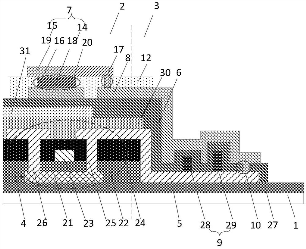
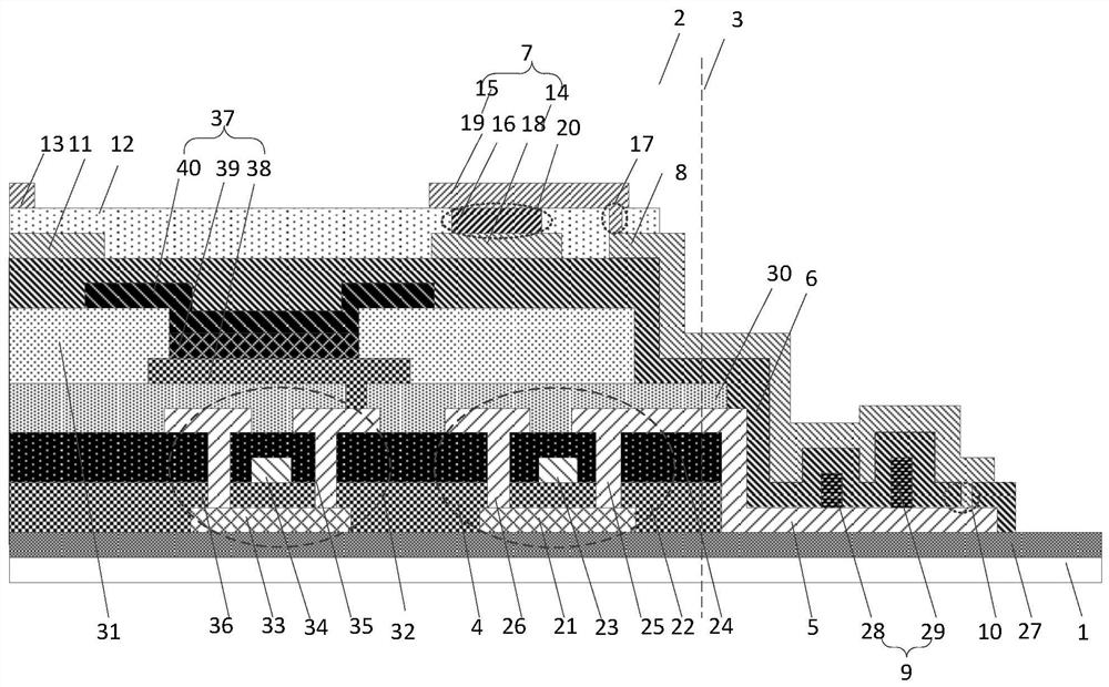
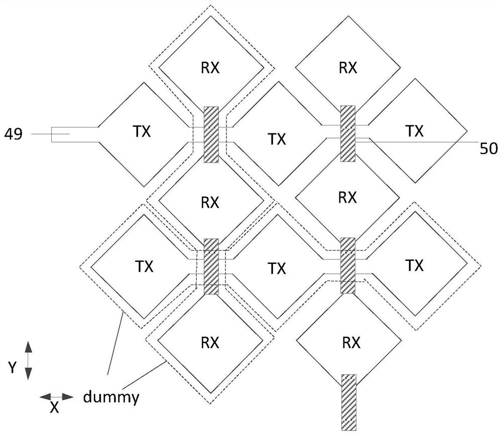
[0050] In order to make the purpose, technical solutions and advantages of the embodiments of the present application clearer, the technical solutions of the embodiments of the present application will be clearly and completely described below in conjunction with the drawings of the embodiments of the present application. Apparently, the described embodiments are some of the embodiments of the present application, but not all of them. And in the case of no conflict, the embodiments in the present application and the features in the embodiments can be combined with each other. Based on the described embodiments of the present application, all other embodiments obtained by persons of ordinary skill in the art without creative efforts shall fall within the protection scope of the present application.

[0051] Unless otherwise defined, the technical terms or scientific terms used in the application shall have the ordinary meanings understood by those skilled in the art to which th...


PUM


Abstract

The invention discloses an array substrate and a preparation method thereof, and a display device, wherein the array substrate is used for reducing grain recognition light propagation paths and improving grain recognition accuracy and efficiency. The array substrate comprises: a substrate body; a display area and a peripheral area, wherein the display area comprises a first thin film transistor onthe substrate, a first connecting lead wore electrically connected with the first thin film transistor on the substrate, a packaging layer located on the first thin film transistor, a photosensitivedevice located on the packaging layer, and a second connecting lead wire located on the packaging layer and electrically connected with the photosensitive device, the first connecting lead wire, the second connecting lead wire and the packaging layer all extend to the peripheral area, the peripheral area comprises a retaining wall positioned between the first connecting lead wire and the packaginglayer, the packaging layer covers the retaining wall, the packaging layer is provided with a first via hole exposing the first connecting lead wire on the side, deviating from the first thin film transistor, of the retaining wall, and the second connecting lead wire is electrically connected with the first connecting lead wire through the first via hole.

Description

technical field [0001] The present application relates to the field of display technology, in particular to an array substrate, a manufacturing method thereof, and a display device. Background technique [0002] Organic light-emitting display devices not only have diversified application fields, but also some products are gradually becoming multi-functional, such as display products with a fingerprint recognition function. At present, optical fingerprint recognition has become one of the most important means of realizing fingerprint recognition of display products. However, in the display products of the prior art, the distance between the optical fingerprint recognition module and the screen surface is relatively long, and the light propagation path is long, which affects the definition of the fingerprint image and affects the accuracy of fingerprint recognition. Contents of the invention [0003] Embodiments of the present application provide an array substrate, a manuf...

Claims


Application Information

Patent Timeline
Patent Type & Authority Applications(China)
IPC IPC(8): H01L27/32H01L21/77G06F3/041G06K9/00
CPCG06F3/0412G06V40/1318H10K59/60H10K59/131H10K59/1201
Inventor 任怀森杨柯侯鹏李岢恒王林林熊登申黄川
Owner BOE TECH GRP CO LTD
Why Eureka
Try Eureka