LED display module and manufacturing method thereof

A technology for display modules and manufacturing methods, applied to electrical components, electrical solid devices, circuits, etc., can solve problems such as uneven color and brightness, uneven light mixing, and uneven thickness of black film layers, and achieve color and brightness Uniform, uniform ink color, uniform light mixing effect

Inactive Publication Date: 2020-12-01
HCP TECH CO LTD
View PDF4 Cites 9 Cited by
  • Summary
  • Abstract
  • Description
  • Claims
  • Application Information

AI Technical Summary

Problems solved by technology

[0004] 1. The uneven mixing of melanin / powder leads to inconsistent ink color between unit boards / modules, as well as uneven color and brightness in different areas of a single unit board / module, especially when viewed from the side;
[0005] 2. When the PCB is deformed, the black film layer will produce uneven film thickness, resulting in uneven light mixing when viewed from the side, and various color cast color block problems;
[0006] 3. Affected by the surface tension of the black film layer material, various random factors lead to different surface shapes at each LED after the film layer is cured, further uneven light mixing

Method used


Image

  • LED display module and manufacturing method thereof
  • LED display module and manufacturing method thereof
  • LED display module and manufacturing method thereof

Examples


Embodiment Construction

[0052] In order to make the purpose, features and advantages of the present invention more obvious and understandable, the technical solutions in the embodiments of the present invention will be clearly and completely described below in conjunction with the accompanying drawings in the embodiments of the present invention. Obviously, the following description The embodiments are only some of the embodiments of the present invention, but not all of them. Based on the embodiments of the present invention, all other embodiments obtained by persons of ordinary skill in the art without making creative efforts belong to the protection scope of the present invention.

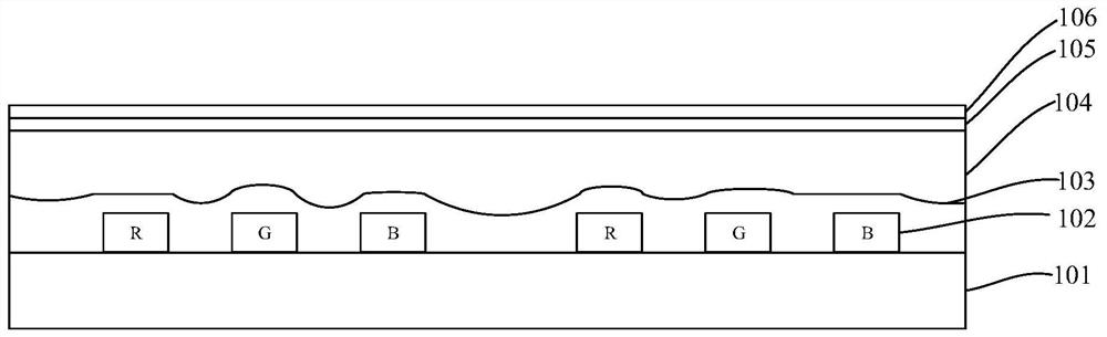
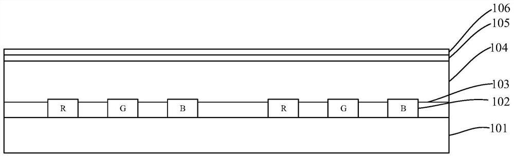
[0053] see figure 2 As shown, this embodiment provides an LED display module, which includes a substrate 101 , the substrate 101 includes a front side and a back side, and a flip-chip LED chip 102 is arranged on the front side. The LED chip 102 generally includes a red LED chip R, a green LED chip G and a blue LED ch...


PUM

PropertyMeasurementUnit
thicknessaaaaaaaaaa

Abstract

The invention discloses an LED display module and a manufacturing method thereof. The manufacturing method comprises the steps: providing a substrate, and enabling LED chips to be disposed on the substrate in an inverted manner; forming a black film layer between the LED chips, and leveling the black film layer through a plasma leveling technology, wherein the black film layer is used for preventing optical crosstalk between the LED chips; and forming a light mixing layer on the black film layer and the LED chip, wherein the light mixing layer is used for protecting the LED chip and the blackfilm layer and providing a light scattering effect for the LED chip. According to the invention, a black film layer is arranged between LED chips, and a light mixing layer is arranged on the black film layer and the LED chip, so that the defects in the prior art can be overcome; and particularly, after the black film layer is flattened through a plasma flattening technology, the ink color betweenunit plates/modules is more uniform and consistent, the colors and brightness of different areas of a single unit plate/module are more uniform, and light mixing is more uniform during side observation.

Description

technical field [0001] The invention belongs to the field of display technology, in particular to an LED display module and a manufacturing method thereof. Background technique [0002] With the continuous development of society and the vigorous advocacy of the country, the LED industry has become one of the most active industries today, and LED display products have gradually entered various fields of social life. At the same time, with the innovation and development of LED display technology, the small-pitch seamless connection LED display module with high resolution per unit area has become the mainstream product of LED display, which can display higher-definition graphics and images. Video can also display more video and image images, especially in the application of image stitching, which can achieve seamless and arbitrary large-area stitching. [0003] At present, one packaging method of LED display is to use COB (Chip on Board) technology to bond R, G, and B three-co...

Claims


Application Information

Patent Timeline
Patent Type & Authority Applications(China)
IPC IPC(8): H01L33/58H01L33/56H01L25/075
CPCH01L25/0753H01L33/56H01L33/58H01L2933/005H01L2933/0058H01L2933/0091
Inventor 庄文荣朱发明卢敬权
Owner HCP TECH CO LTD
Why Eureka
Try Eureka