
Processing technology of conductive foam and conductive foam

A technology of conductive foam and processing technology, applied in the field of conductive foam, can solve problems such as easy breakage of conductive materials, and achieve the effects of not easy to break, speeding up efficiency, and reducing processing time

Active Publication Date: 2020-12-04
SHENZHEN HFC SHIELDING PRODS CO LTD
View PDF8 Cites 3 Cited by
  • Summary
  • Abstract
  • Description
  • Claims
  • Application Information

AI Technical Summary

Problems solved by technology

[0003] In view of the above-mentioned related technologies, the inventor believes that there is a defect that the conductive material is prone to fracture when cutting the foam coated with the conductive material

Method used


Image

  • Processing technology of conductive foam and conductive foam
  • Processing technology of conductive foam and conductive foam
  • Processing technology of conductive foam and conductive foam

Examples


Embodiment 1

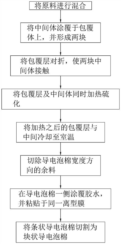
[0045] Example 1: as figure 1 As shown, including providing a cladding layer 1 and raw materials, the cladding layer 1 is conductive material such as conductive cloth, copper, aluminum foil, tin-plated PI, gold-plated PI, etc. Environmentally friendly flame retardants, pigments, catalysts and retarders, the weight ratio is 0.7:0.19:0.05:0.029:0.02:0.01:0.001, the raw materials are mixed and stirred to form Intermediate 3, stirred for 60 seconds to 120 seconds, and stirred temperature below 30 degrees Celsius;

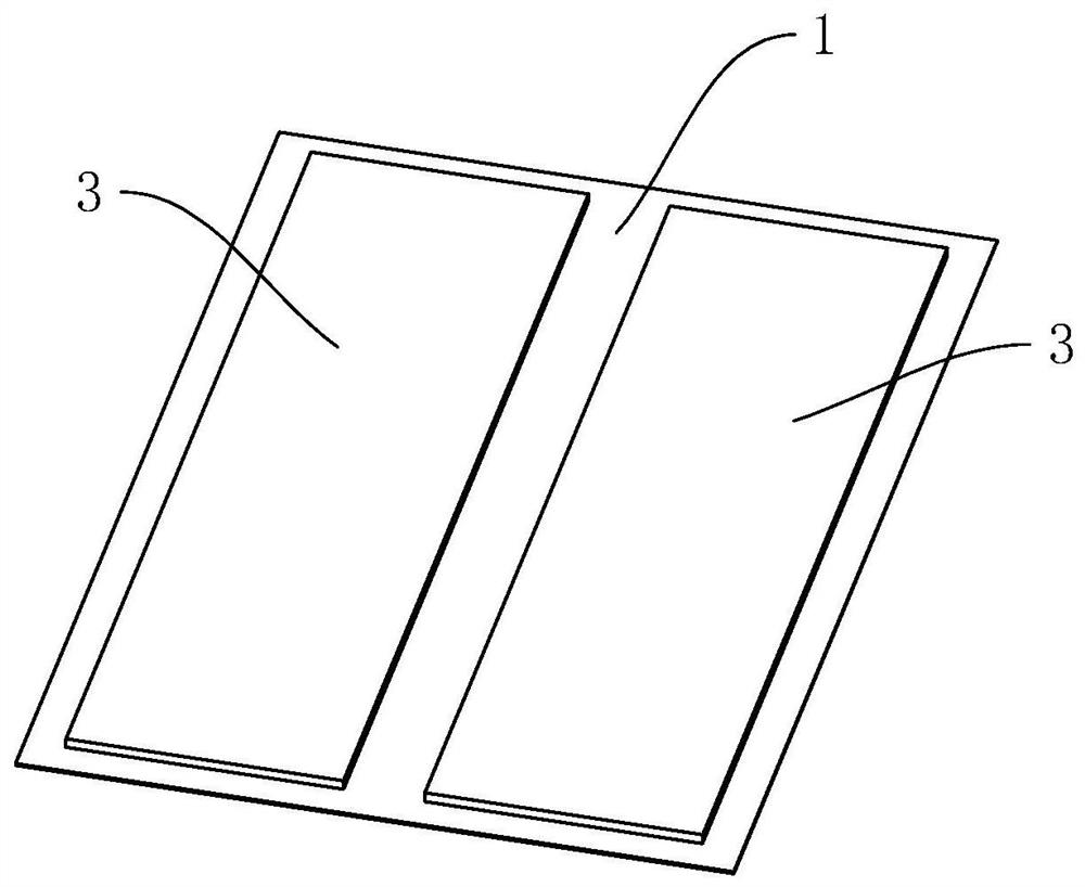
[0046] like figure 2 As shown, the cladding layer 1 is laid flat with one side facing upward, and the intermediate 3 is coated on the upper end face of the cladding layer 1, and the coating thickness is one third of the required thickness of the elastic layer 2, and The coated intermediate 3 is formed into two pieces and a gap is left between the two intermediate bodies 3, and a gap is left between the coated intermediate 3 and the vertical sidewall of the cladding l...

Embodiment 2

[0053] Example 2: as Image 6 As shown, the difference from Example 1 is that when the intermediate body 3 is coated, the widths of the two coated intermediate bodies 3 along the width direction of the cladding layer 1 are different;

[0054] like Figure 7 As shown, when trimming the conductive foam, trim the side wall of the elastic layer 2 in contact with the covering layer 1, so that the side wall of the elastic layer 2 is not in contact with the covering layer 1, and the covering layer 1 The side walls close to the conductive foam are in the same plane;

[0055]When the glue 4 is applied, the glue 4 is applied to the position where the elastic layer 2 is in contact with the covering layer 1 but is not completely covered by the covering layer 1 .

[0056] At this time, the required thickness of the glue 4 is reduced, so that the conductive foam can be used for buffering between electronic products with smaller gaps under the condition that the overall thickness of the co...


PUM


Abstract

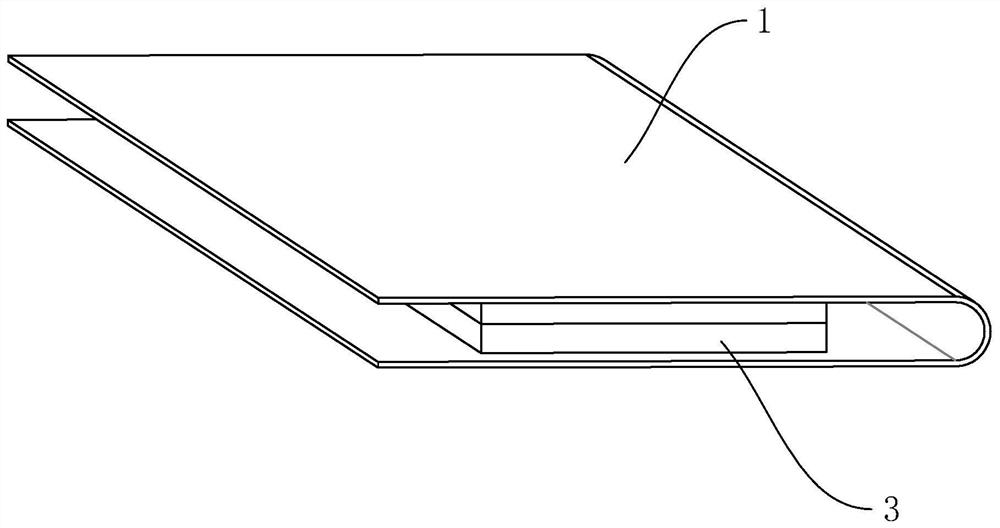
The invention relates to a processing technology of conductive foam and conductive foam, and the technology comprises the steps: providing a coating layer and raw materials, mixing the raw materials,and stirring the raw materials to form an intermediate; flatly laying the coating layer, coating the upper end surface of the coating layer with two intermediates, reserving a gap between the two intermediates, and reserving a gap between the intermediates and the edge of the coating layer; folding the coating layer along the position between the two intermediates, so that the intermediates located on the two sides of the bent position of the coating layer make contact with each other; putting the folded coating layer into a jig, heating and vulcanizing the jig, the coating layer and the intermediate, heating the intermediate to form an elastic layer, and adhering the elastic layer to the coating layer to form conductive foam; and simultaneously cooling the elastic layer and the coating layer to room temperature. The intermediate is directly bonded with the coating layer in the process of foaming the intermediate into the elastic layer, and a gap is not easy to generate between the elastic layer and the coating layer, so that a conductive medium of the coating layer is not easy to break in the subsequent cutting process of the conductive foam.

Description

technical field [0001] The present application relates to the technical field of conductive foam, in particular to a processing technology of conductive foam and conductive foam. Background technique [0002] At present, in the production process of conductive foam, the foam is usually cut to the required size first, and then the conductive material is wrapped around the foam to make the conductive material adhere to the outer wall of the foam. The foam cut sections of the conductive material are in the desired size. [0003] With regard to the above-mentioned related art, the inventor believes that there is a defect that the conductive material is easily broken when the foam covered with the conductive material is cut. [0004] Therefore, it is necessary to propose a new technical solution to solve the above problems. SUMMARY OF THE INVENTION [0005] In order to prevent gaps between the foam and the covering layer when they are connected, and to prevent the conductive ...

Claims


Application Information

Patent Timeline
Patent Type & Authority Applications(China)
IPC IPC(8): C09J7/26C09J7/29C09J7/30
CPCC09J7/26C09J7/29C09J7/30C09J2475/00C09J2400/243
Inventor 窦兰月张延赵园园廖如雪
Owner SHENZHEN HFC SHIELDING PRODS CO LTD
Learn More