Method and system for establishing semiconductor defect scanning program
A technology for defect scanning and method establishment, which is applied in the field of semiconductor manufacturing and can solve the problems of consuming human resources and engineering time
- Summary
- Abstract
- Description
- Claims
- Application Information
AI Technical Summary
Problems solved by technology
Method used
Image


Examples
no. 1 example
[0037] In the first embodiment, a method for establishing a semiconductor defect scanning program includes the following steps:
[0038] S1, select the process platform and process flow;
[0039] S2, under the above process platform and process flow, select the benchmark product;
[0040] S3, collect defect scanning program data after different process levels of the benchmark product, and establish a database;
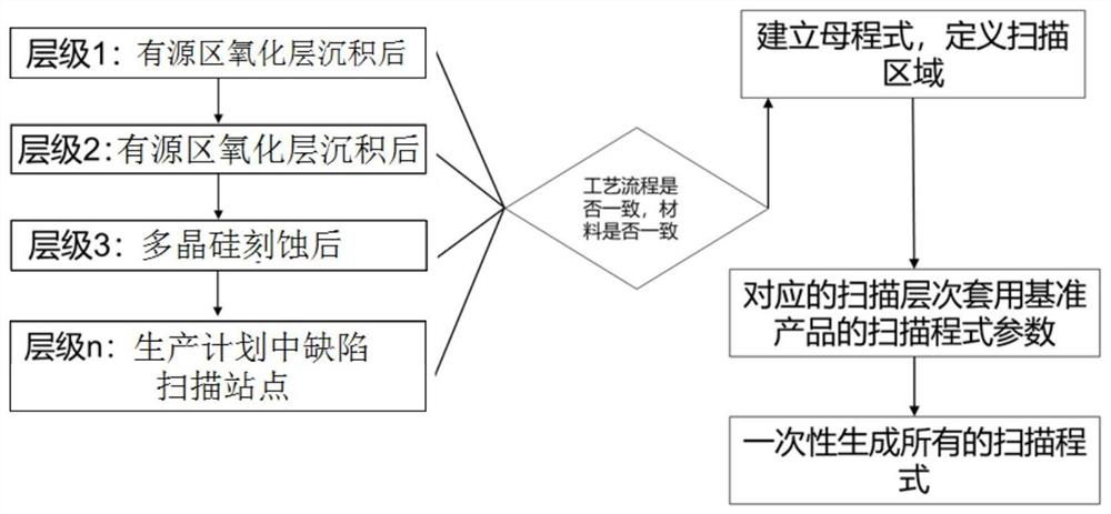
[0041] S4, comparing the process platform, process flow and corresponding material parameters of the new product with the process platform, process flow and corresponding material parameters of the benchmark product;
[0042] If there is no difference, after defining the defect scanning area for the new product, use the defect program parameters of the corresponding level of the benchmark product to create a new product scanning program at one time;
[0043] If there is a difference, the new product is used as the benchmark product to establish a database.
[0044] ...
no. 2 example
[0045] In the second embodiment, a method for establishing a semiconductor defect scanning program includes the following steps:
[0046]S1, select the process platform and process flow;
[0047] S2, under the above process platform and process flow, select the benchmark product;
[0048] S3, collect defect scanning program data after different process levels of the benchmark product, and establish a database;
[0049] The area and level of defect scanning can be selected as follows;
[0050] After the oxide layer in the active area is deposited, the acquisition process parameters include: incident light intensity, focusing value, contrast window size, training light intensity of each scanning area, and signal-to-noise ratio designated as a defect;
[0051] After the active area is etched, the acquisition process parameters include: incident light intensity, focusing value, contrast window size, training light intensity of each scanning area, and signal-to-noise ratio design...
no. 3 example
[0057] In the third embodiment, the present invention provides a system for establishing a semiconductor defect scanning program, which can be integrated into a defect scanning machine using computer programming technology, including:
[0058] Selection module, which is used to select the selection process platform and process flow of semiconductor devices, and select the benchmark product under the above process platform and process flow;
[0059] A collection module, which is used to collect defect scanning program data after different process levels of the benchmark product, and establish a database;
[0060] A comparison module, which is used to compare the process platform, process flow and corresponding material parameters of the new product with the process platform, process flow and corresponding material parameters of the benchmark product;
[0061] A program building module, which determines whether to create a new product scanning program according to the comparison...
PUM
 Abstract
Description
Claims
Application Information
 - R&D
- Intellectual Property
- Life Sciences
- Materials
- Tech Scout
- Unparalleled Data Quality
- Higher Quality Content
- 60% Fewer Hallucinations
Browse by: Latest US Patents, China's latest patents, Technical Efficacy Thesaurus, Application Domain, Technology Topic, Popular Technical Reports.
© 2025 PatSnap. All rights reserved.Legal|Privacy policy|Modern Slavery Act Transparency Statement|Sitemap|About US| Contact US: help@patsnap.com