A kind of micro LED module and preparation method thereof

A technology of quantum dots and quantum wells, which is applied in the field of MicroLED modules and their preparation, can solve the problems of great influence of brightness, color shift, and large temperature change of luminous characteristics, and achieves good waterproofing, sealing and anaerobicity, and high luminous efficiency. Effect

Active Publication Date: 2021-11-05
HCP TECH CO LTD
View PDF0 Cites 0 Cited by
  • Summary
  • Abstract
  • Description
  • Claims
  • Application Information

AI Technical Summary

Problems solved by technology

However, Micro LED technology still has the following problems: When Micro LED is used for display, it needs to work in a small current range, the main range is 0.02-2A / cm 2 , in this small current range, the dislocation density inside the epitaxial layer of the chip has a great influence on the brightness, which may easily lead to uneven brightness or even no brightness.
However, in the current quantum dot luminescence technology, such as CdSe, which contains the highly toxic element Cd, which has been banned in many countries, its luminescence characteristics also vary greatly with temperature, and there is a problem of color shift.

Method used


Image

  • A kind of micro LED module and preparation method thereof
  • A kind of micro LED module and preparation method thereof
  • A kind of micro LED module and preparation method thereof

Examples


Embodiment 1

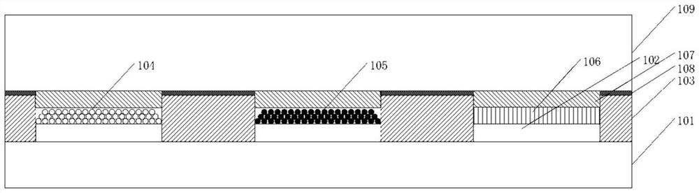
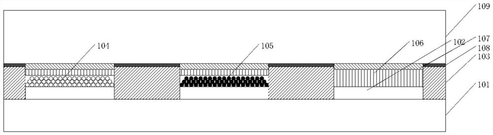
[0050] see figure 1As shown, this embodiment provides a Micro LED module, including a gallium nitride single crystal substrate 101, on which a quantum well light-emitting layer 102 is formed, and the quantum well light-emitting layer 102 is n-type doped. Red quantum dots 104 and green quantum dots 105 are also arranged on the well light-emitting layer 102 .

[0051] Specifically, a hole injection layer 107 is further provided on the quantum well light emitting layer 102 .

[0052] Further, the gallium nitride single crystal substrate 101 is an n-type single crystal substrate; or the gallium nitride single crystal substrate 101 is a non-doped substrate on which n-type gallium nitride is epitaxially formed.

[0053] In this embodiment, the substrate is a gallium nitride single crystal substrate 101, and the Micro LED epitaxially on it has a low dislocation density, has a lower impact on brightness, and has a higher luminous efficiency, so that the Micro LED can operate in a sma...

Embodiment 2

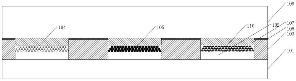
[0064] see image 3 As shown, this embodiment provides a Micro LED module, the quantum well light-emitting layer 102 is a GaN:Si / AlGaN:Si superlattice quantum well, and the quantum well light-emitting layer 102 not only has red quantum dots 104 and green quantum dots 105, blue quantum dots 110 are also provided. The red quantum dots 104, the green quantum dots 105, and the blue quantum dots 110 are perovskite quantum dots.

[0065] It should be noted that this embodiment includes a gallium nitride single crystal substrate 101, an n-type doped quantum well light-emitting layer 102, a black matrix 103, red quantum dots 104, green quantum dots 105, blue quantum dots 110, A hole injection layer 107 , a thin film transistor array 108 and a glass cover 109 .

[0066] In the Micro LED module provided in this embodiment, the substrate is a gallium nitride single crystal substrate 101, and the Micro LED epitaxial on it has a low dislocation density, lower influence on brightness, and...

Embodiment 3

[0069] This embodiment provides a method for preparing a Micro LED module, which can be used to prepare the Micro LED module provided in the above embodiment, which specifically includes the following steps:

[0070] 1. Provide a gallium nitride single crystal substrate 101, form a quantum well light emitting layer 102 thereon, and pattern the quantum well light emitting layer 102;

[0071] 2. Forming a black matrix 103 on the gallium nitride single crystal substrate 101;

[0072] 3. Forming quantum dots of at least one color on the quantum well light-emitting layer 102;

[0073] 4. Form a hole injection layer 107 on the quantum dots.

[0074] In the method for preparing a Micro LED module provided in this embodiment, the substrate is a gallium nitride single crystal substrate 101, and the Micro LED epitaxially thereon has a low dislocation density, lower influence on brightness, and higher luminous efficiency , so that the Micro LED can still emit uniform light with suffici...


PUM


Abstract

The invention discloses a Micro LED module and a preparation method thereof. The substrate is a single crystal substrate, and the Micro LED epitaxial thereon has a low dislocation density, lower influence on brightness, and higher luminous efficiency, so that Micro LED can still emit uniform light with sufficient brightness in the small current range; the quantum well light-emitting layer is n-type doped, and the perovskite quantum dot is a semiconductor material, which can effectively realize hole injection through the perovskite, so that the quantum well light-emitting layer Light up and excite the perovskite quantum dots on it to make it emit light of other colors, complete color conversion, and realize full-color Micro LED modules; perovskite quantum dots have better temperature stability, which can ensure the color of the display module Stability; moreover, the quantum dots are arranged on the quantum well light-emitting layer, and are located under the hole injection layer and the glass cover plate, which has better waterproof and oxygen-proof effects.

Description

technical field [0001] The invention belongs to the field of display technology, and in particular relates to a Micro LED module and a preparation method thereof. Background technique [0002] In the application of LED chips, the application of ordinary LED chips is mainly in lighting and display backlight modules, and the current rapid development of Mini LED is mainly applied in indoor and outdoor display screens. But in many applications that require higher size and pixel density, the existing technology cannot meet the requirements. Therefore, Micro LED technology emerged as a brand-new display technology. Its application concept is completely different from the previous two. It can be applied in wearable watches, mobile phones, car displays, VR / AR, TVs and other fields. The ultimate display technology. [0003] Micro LED has advantages in brightness, contrast, response speed, color gamut, lifespan, energy consumption, etc. From the perspective of technology iteration...

Claims


Application Information

Patent Timeline
Patent Type & Authority Patents(China)
IPC IPC(8): H01L33/02H01L33/50H01L33/52H01L27/15H01L33/00
CPCH01L27/15H01L33/0075H01L33/02H01L33/50H01L33/52H01L2933/0041H01L2933/005
Inventor 庄文荣卢敬权
Owner HCP TECH CO LTD
Why Eureka
Try Eureka