Surface-modified light-emitting chip and preparation method thereof

A light-emitting chip and surface modification technology, applied in electrical components, circuits, semiconductor devices, etc., can solve problems such as inability to apply, achieve good luminous uniformity, uniform luminosity or surface illuminance, and reduce visual defects.

Pending Publication Date: 2020-12-11
李宛儒
View PDF0 Cites 0 Cited by
  • Summary
  • Abstract
  • Description
  • Claims
  • Application Information

AI Technical Summary

Problems solved by technology

[0003] Because the diffuser, lens and light-emitting chip must maintain an appropriate distance, the lens and diffuser can effectively play the role of atomization to make the light uniform, and the lens itself has a certain thickness, so the panel containing the light-emitting chip, lens and diffuser The thickness of the backlight device or lighting device is usually greater than 3 cm, which cannot be applied to advanced thin design panel electronic products or lighting devices

Method used


Image

  • Surface-modified light-emitting chip and preparation method thereof

Examples


no. 1 example

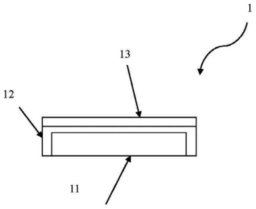
[0021] According to the first embodiment of the present invention, the present invention provides a surface-modified light-emitting chip, which includes a light-emitting chip and a diffusion adhesive layer; and the diffusion adhesive layer covers the front top of the light-emitting chip, thereby forming the described Surface-modified light-emitting chip.

[0022] In one embodiment, the manufacturing implementation of the light-emitting chip includes wafer-level packaging, melting luminescent glue, dispensing, lamination of luminescent film or a combination thereof.

[0023] The following are examples of surface-modified light-emitting chips produced by wafer-level packaging.

[0024] In one embodiment, the wafer-level package is coated with a luminescent powder layer on the surface of the chip.

[0025] In one embodiment, the luminescent powder layer includes polymer glue, silica gel, epoxy resin or a combination thereof

[0026] In one embodiment, the luminescent powder lay...


PUM

PropertyMeasurementUnit
transmittivityaaaaaaaaaa

Abstract

The invention provides a surface-modified light-emitting chip. The surface-modified light-emitting chip comprises a light-emitting chip and a diffusion adhesive layer, and the diffusion glue layer covers the top of the front surface of the light-emitting chip so as to form the surface-modified light-emitting chip. The preparation method of the surface-modified light-emitting chip comprises a powder attachment procedure. The invention at least has the technical effects that: the diffusion glue layer is used for covering the top of the front surface of the light source to achieve a self-atomization effect; the visual defect that bright spots are generated on the light-emitting surface is directly reduced, and five-surface light emission is maintained to enable the light-emitting surface to have uniform luminosity or surface illuminance.

Description

technical field [0001] The invention relates to a surface-modified light-emitting chip and a preparation method thereof. In particular, the above-mentioned surface-modified light-emitting chip is a light-emitting chip modified with a diffusion glue layer on the top of the front surface. Background technique [0002] The light-emitting chips (LEDs) used in TV panel backlight devices and planar lighting devices emit light from the top in one direction (the light emitting angle is 120 degrees), which will produce bright spots. Therefore, it is necessary to use lenses to enlarge the optical angle and reduce the top bright spots. At the same time, add a diffuser panel Strengthen the atomization effect of the lens to achieve the effect of uniform light output and consistent surface illumination. [0003] Because the diffuser, lens and light-emitting chip must maintain an appropriate distance, the lens and diffuser can effectively play the role of atomization to make the light uni...

Claims


Application Information

Patent Timeline
Patent Type & Authority Applications(China)
IPC IPC(8): H01L33/58H01L33/44
CPCH01L33/44H01L33/58H01L2933/0025H01L2933/0058
Inventor 李宛儒
Owner 李宛儒
Why Eureka
Try Eureka