Photoluminescent wafer as well as preparation method and application thereof

A technology of photoluminescence and wafers, which is applied in chemical instruments and methods, crystal growth, self-solidification, etc., can solve the problem of rising chip temperature, affecting the service life of the fluorescent powder layer, reducing the light efficiency of the light-emitting layer, etc. question

Inactive Publication Date: 2011-08-03
ZHEJIANG SHENDU LIGHTING
View PDF9 Cites 15 Cited by
  • Summary
  • Abstract
  • Description
  • Claims
  • Application Information

AI Technical Summary

Problems solved by technology

In this process, it is easy to mix harmful impurities, destroy the integrity of the crystal lattice, and reduce the luminous efficiency;
[0008] 2. The powder phosphor needs to be mixed with a binder and coated on the light-emitting diode chip. When the binder is mixed, it is very easy to contaminate the fluorescent crystal; Refraction and reflection (scattering) will inevitably occur when the powder crystal is used, and the reflected light will be absorbed when it passes through the binder, reducing the light effect of the light-emitting layer; at the same time, because the thermal conductivity of the binder is much lower than that of the fluorescent crystal (epoxy The thermal conductivity of the resin is only 0.2W / m / K), and it is easy to cause the temperature of the chip to rise when it is coated on the power chip, which will not only reduce the light efficiency of the chip, but also affect the light efficiency of the phosphor itself and the entire Lifetime of Phosphor Layer

Method used


Image

  • Photoluminescent wafer as well as preparation method and application thereof
  • Photoluminescent wafer as well as preparation method and application thereof
  • Photoluminescent wafer as well as preparation method and application thereof

Examples


Embodiment 1

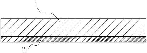
[0077] like Figure 5 As shown, the raw material Y with a purity higher than 4N is selected 2 O 3 , Tb 4 O 7 , Dy 2 O 3 , CeO 2 , Al 2 O 3 , press (Y 0.60 Tb 0.26 Dy 0.20 Ce 0.04 ) 3 Al 5 O 12 The stoichiometric ratio is weighed and mixed. 1.4% cosolvent BaF based on the total weight of the mixture 2 and 0.1% H 3 BO 3 , compression molding, burning at 900 ° C for 2h to shrink the volume and then placing it in the iridium crucible 7, heating to 1970 ° C in the high-frequency induction furnace 8 of the single mold 11 melt casting equipment in an argon atmosphere, and melting at 1980 ~ 1990 ℃ superheated temperature for 8min. Under the pressure of 20 mmHg, the melt flows through the crucible mouth slit 9 to a single mold 11 with a distance of 0.2 mm from the lip 10 and a moving speed of 8.2 m / s to form a polycrystalline photoluminescent wafer 1 with a thickness of 30 μm. like figure 1 shown, SiO was then deposited by high-frequency reactive sputtering 2T...

Embodiment 2

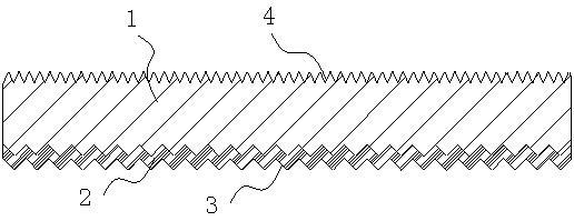
[0079] like Image 6 As shown, the raw material Y with a purity higher than 4N is selected 2 O 3 ,Gd 2 O 3 , CeO 2 , Al 2 O 3 , Ga 2 O 3 , press (Y 0.72 Gd 0.26 Ce 0.02 ) 3 (Al 0.80 Ga 0.20 ) 5 O 12 The stoichiometric ratio is weighed and mixed. Then mix in 0.2% of cosolvent H based on the total weight of the above mixture 3 BO 3 , compression molding, after burning at 900 ° C for 2h to shrink the volume, it is placed in an iridium crucible 7, heated to 1970 ° C in an argon atmosphere in a high-frequency induction furnace 8 of a single mold melt casting equipment, and melted at 1980 ~ 1990 ℃ superheat temperature, keep for 10min. Under the pressure of 20mmHg, the melt flows through the crucible mouth slit 9 to a single mold 11 with a distance of 0.2mm from the lip 10 and a moving speed of 6.4m / s to form a polycrystalline photoluminescent wafer 1 with a thickness of 46µm. like Image 6 As shown, the single mold 11 is engraved with punches 12 arranged in...

Embodiment 3

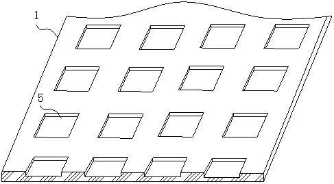
[0081] like Figure 7 , Figure 8 As shown, the raw material Y with a purity higher than 4N is selected 2 O 3 , CeO 2 , Tb 4 O 7 , Pr 6 O 11 , Al 2 O 3 , press (Y 0.54 Tb 0.40 Ce 0.04 Pr 0.02 ) 3 Al 5 O 12 The stoichiometric ratio is weighed and mixed. 1.4% of cosolvent H based on the total weight of the above mixture was mixed 3 BO 3 , compression molding, burning at 900 ° C for 2h to shrink the volume and then placing it in an iridium crucible 7, heated to 1970 ° C in an argon atmosphere in a high-frequency induction furnace 8 of a double mold melt casting equipment, and melted at 1980 ~ 1990 ℃ superheat temperature, keep for 10min. Under the pressure of 20 mmHg, the melt flows through the slits of the crucible mouth 9 at the lower part of the iridium crucible 7 and flows through the slits of the two counter-rotating casting molds 13 to form molten pools and solidify into wafers. The distance from the crucible mouth lip 10 to the narrowest point of the...


PUM

PropertyMeasurementUnit
thicknessaaaaaaaaaa
sizeaaaaaaaaaa
thicknessaaaaaaaaaa

Abstract

The invention relates to the manufacturing field of light emitting diodes (LED), in particular to a photoluminescent wafer for the LED as well as preparation method and application thereof. The photoluminescent wafer is a slice-shaped crystal in a garnet structure with a general formula of A3B5O12 without doping any resins and other bonding agents, the thickness of the photoluminescent wafer is not less than 20 um, and the size of the crystal particle is not less than 10 um; moreover, the photoluminescent wafer comprises a first element A, a second element B and an active element, wherein thefirst element A is at least one of rare-earth elements Y, Lu, La, Gd or Sm; the second element B is at least one of the elements Al, Ga or In; and the active element is at least one of the rare-earthelements Ce, Pr, Tb and Dy. The photoluminescent wafer has the characteristics of high light emitting efficiency and good light emitting uniformity; the light transmission of the light emitting layercan not be reduced by light adsorption of the bonding agent; and the surface of the photoluminescent wafer is easy for people to carry out various optical treatments.

Description

technical field [0001] The invention relates to the field of light-emitting diode (LED) manufacturing, in particular to a photoluminescence wafer used for LED and its preparation method and application. Background technique [0002] Power LEDs will gradually replace some traditional lighting sources and become a new generation of lighting products. At present, the main problem of LED lighting products is the high cost and price, and the luminous efficiency, light color and service life need to be further improved, and these problems are all closely related to the phosphor materials of LEDs currently used for white lighting. Now this kind of fluorescent powder mostly uses yellow fluorescent powder materials such as yttrium aluminum garnet (YAG) of Nichia Chemical Company of Japan and terbium-garnet (TAG) of Osram Company. [0003] As early as 1964, the yttrium aluminum garnet crystal material for solid-state lasers was prepared, and then scientists from various countries hav...

Claims


Application Information

Patent Timeline
Patent Type & Authority Applications(China)
IPC IPC(8): C30B29/28C30B11/00C30B15/00H01L33/48H01L33/00H01L25/075
CPCH01L2224/48091H01L2224/48247H01L2224/49107
Inventor 陈哲艮
Owner ZHEJIANG SHENDU LIGHTING
Why Eureka
Try Eureka