Epitaxial preparation method of P type heavily-doped silicon carbide film by controlling flow rate of hydrogen gas

A technology of silicon carbide and heavy doping, which is applied in chemical instruments and methods, gaseous chemical plating, and from chemically reactive gases, etc., can solve problems affecting device performance, high bond strength of silicon carbide, and lattice damage, etc., to achieve Simplification of preparation process, improvement of device performance, and effect of crystal lattice integrity

Inactive Publication Date: 2014-12-24
XIDIAN UNIV
View PDF4 Cites 1 Cited by
  • Summary
  • Abstract
  • Description
  • Claims
  • Application Information

AI Technical Summary

Problems solved by technology

However, due to the high bond strength of silicon carbide, the doping in the device manufacturing process cannot use the diffusion process, and can only be controlled by epitaxy and high-temperature ion implantation.
High-temperature ion implantation will cause a lot of lattice damage and form a large number of lattice defects, which are difficult to completely eliminate even with annealing, seriously affecting the performance of the device, and the efficiency of ion implantation is very low, so it is not suitable for large-area doping

Method used


Image

  • Epitaxial preparation method of P type heavily-doped silicon carbide film by controlling flow rate of hydrogen gas

Examples


Embodiment 1

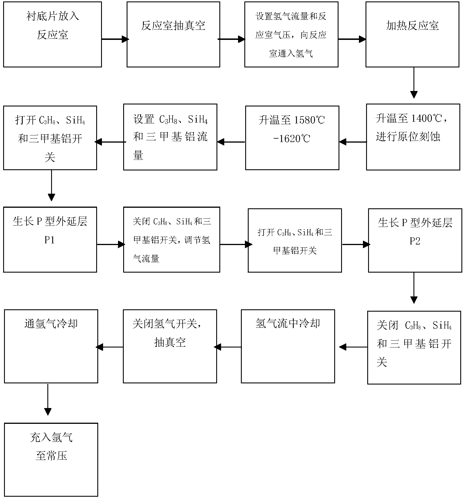
[0020] Step 1, placing the silicon carbide substrate into the reaction chamber of the silicon carbide CVD equipment.

[0021] (1.1) Selection bias A 4H silicon carbide substrate with a crystal orientation of 4° is placed in the reaction chamber of the silicon carbide CVD equipment;

[0022] (1.2) Vacuumize the reaction chamber until the pressure in the reaction chamber is lower than 1×10 -7 mbar.

[0023] Step 2, heating the reaction chamber in the hydrogen flow.

[0024] (2.1) Open the hydrogen switch leading to the reaction chamber, and control the hydrogen flow to gradually increase to 60L / min;

[0025] (2.2) Turn on the vacuum pump to extract the gas in the reaction chamber, and keep the pressure in the reaction chamber at 100mbar;

[0026] (2.3) Gradually increase the power of the heating source to slowly increase the temperature of the reaction chamber.

[0027] Step 3, performing in-situ etching on the substrate.

[0028] (3.1) When the temperature of the reactio...

Embodiment 2

[0042] Step 1, placing the silicon carbide substrate into the reaction chamber of the silicon carbide CVD equipment.

[0043] (1.1) Selection bias A 4H silicon carbide substrate with a crystal orientation of 8° is placed in the reaction chamber of the silicon carbide CVD equipment;

[0044] (1.2) Vacuumize the reaction chamber until the pressure in the reaction chamber is lower than 1×10 -7 mbar.

[0045] Step 2, heating the reaction chamber in the hydrogen flow.

[0046] (2.1) Open the hydrogen switch leading to the reaction chamber, and control the hydrogen flow to gradually increase to 60L / min;

[0047] (2.2) Turn on the vacuum pump to extract the gas in the reaction chamber, and keep the pressure in the reaction chamber at 100mbar;

[0048] (2.3) Gradually increase the power of the heating source to slowly increase the temperature of the reaction chamber.

[0049] Step 3, performing in-situ etching on the substrate.

[0050] (3.1) When the temperature of the reaction ...


PUM


Abstract

The invention relates to an epitaxial preparation method of a P type heavily-doped silicon carbide film by controlling a flow rate of a hydrogen gas. The preparation method comprises the following steps: (1) placing a silicon carbide substrate into a reaction chamber of silicon carbide CVD (chemical vapor deposition) equipment, and vacuating the reaction chamber; (2) introducing H2 into the reaction chamber until the gas pressure of the reaction chamber reaches 100mbar, keeping the gas pressure of the reaction chamber constant, gradually increasing the flow rate of the H2 to 60 L / min, and continuously introducing H2 into the reaction chamber; (3) switching on a high-frequency coil induction heater RF, gradually increasing the power of the heater, and carrying out in-situ etching when the temperature of the reaction chamber is greatly increased to 1400 DEG C; and (4) keeping the temperature and the pressure intensity constant while the temperature of the reaction chamber is 1580-1600 DEG C, and introducing C3H8 and SiH4 into the reaction chamber; placing liquid-state trimethyl aluminum into a bubbler as a doping source, introducing a certain amount of H2 into the bubbler and introducing the H2 into the reaction chamber along with the trimethyl aluminum.

Description

technical field [0001] The invention belongs to the technical field of semiconductor device manufacturing, and in particular relates to a method for preparing a P-type gradient doped silicon carbide epitaxial layer by utilizing the existing MOCVD growth process of silicon carbide material. Background technique [0002] Silicon carbide has the advantages of wide band gap, high thermal conductivity, high breakdown strength, high electron saturation drift velocity, high hardness, etc., and also has strong chemical stability. These excellent physical and electrical properties make silicon carbide have many advantages in application. The forbidden band allows silicon carbide intrinsic carriers to maintain a low concentration at high temperatures, so it can work at very high temperatures. The high breakdown field strength enables silicon carbide to withstand high electric field strength, which allows silicon carbide to be used to make high-voltage, high-power semiconductor device...

Claims


Application Information

Patent Timeline
Patent Type & Authority Applications(China)
IPC IPC(8): C30B25/16C30B29/36C23C16/455C23C16/52C23C16/32
Inventor 王悦湖胡继超张艺蒙宋庆文张玉明
Owner XIDIAN UNIV
Why Eureka
Try Eureka