Light emitting diode encapsulating structure and manufacturing method thereof

A technology of light-emitting diodes and packaging structures, which is applied to semiconductor devices, electrical components, circuits, etc., can solve the problems of reducing production efficiency, increasing production costs, and affecting the light uniformity of light-emitting diode packaging structures, and achieves the effect of optimal light uniformity

Inactive Publication Date: 2010-09-22
EVERLIGHT ELECTRONICS
View PDF4 Cites 13 Cited by
  • Summary
  • Abstract
  • Description
  • Claims
  • Application Information

AI Technical Summary

Problems solved by technology

However, since the encapsulant contains fluorescent material, during the process of waiting for baking, the fluorescent material will settle due to the long time that the encapsulant is filled in the cavity of the chip or the timing of filling the glue is different, resulting in the generation of fluorescent material. The phenomenon of uneven distribution (that is, most of the fluorescent materials settle on the bottom surface of the chip cavity or the chip surface), and only a small part of the fluorescent materials are scattered in the encapsulation body, which in turn affects the light output of the produced LED packaging structure Evenness
[0004] In addition, since the shapes of the carriers of the known light emitting diode packaging structure are different, if the fluorescent layer is formed on the light emitting diode chip by means of fluorescent coating process, the machine equipment must be adjusted for different carriers, thus reducing the production efficiency and increase production cost

Method used


Image

  • Light emitting diode encapsulating structure and manufacturing method thereof
  • Light emitting diode encapsulating structure and manufacturing method thereof
  • Light emitting diode encapsulating structure and manufacturing method thereof

Examples


Embodiment Construction

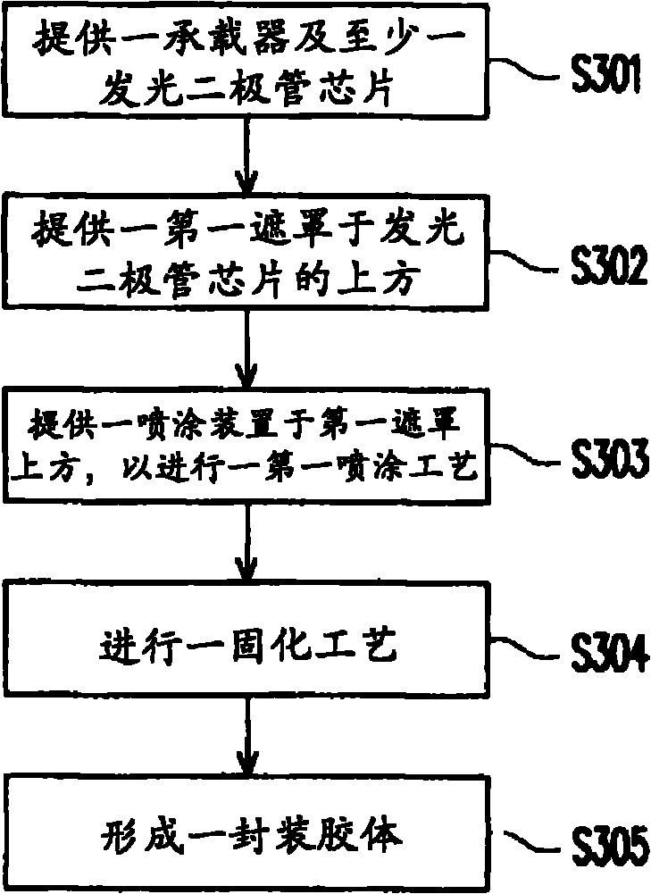
[0052] In order to make the above-mentioned features and advantages of the present invention more comprehensible, the following specific embodiments are described in detail together with the accompanying drawings.

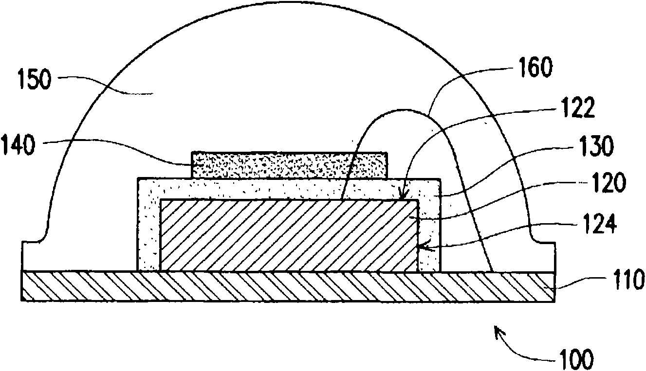
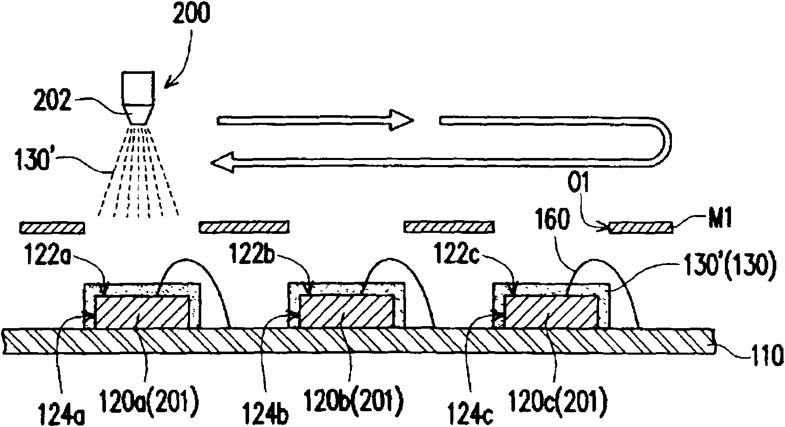
[0053] figure 1 It is a schematic cross-sectional view of a light emitting diode packaging structure according to an embodiment of the present invention. Please refer to figure 1 , in this embodiment, the LED packaging structure 100 includes a carrier 110 , a LED chip 120 , a first phosphor layer 130 , a second phosphor layer 140 and an encapsulant 150 .

[0054] In detail, the LED chip 120 is disposed on the carrier 110, and the LED chip 120 has a light-emitting surface 122 and a plurality of side surfaces 124 connected to the light-emitting surface 122, wherein the LED chip 120 passes through at least one wire 160 ( figure 1 Only one of them is schematically shown) is electrically connected to the carrier 110 . In this embodiment, the carrier 110 is, for examp...


PUM


Abstract

The invention discloses a manufacturing method of a light emitting diode encapsulating structure, which provides a loader and at least one light emitting diode chip which is provided with a light outlet surface and a plurality of side surfaces. The invention provides a first shade which is provided with at least one first opening; and the first opening at least exposes out of the light emitting diode chip. A spray coating device is arranged above the first shade for carrying out a first spray coating technology. The spray coating device is used for carrying out reciprocating spray coating on first fluorescent solution along a route so that the light outlet surface and the side surfaces of the light emitting diode chip are coated conformally by the first fluorescent solution. A first curing technology is carried out for curing the first fluorescent solution into a first fluorescent layer. An encapsulating colloid is formed for coating the first fluorescent layer and a part of the loader.

Description

technical field [0001] The present invention relates to a semiconductor packaging structure and a manufacturing method thereof, and in particular to a light emitting diode packaging structure and a manufacturing method thereof. Background technique [0002] Light-emitting diodes have advantages such as long life, small size, high shock resistance, low heat generation, and low power consumption, so they have been widely used as indicators or light sources in households and various equipment. In recent years, light-emitting diodes have developed towards multi-color and high brightness, so their application fields have been extended to large outdoor billboards, traffic lights and related fields. In the future, light-emitting diodes may even become the main lighting source with both power saving and environmental protection functions. [0003] It is known that since the packaging structure of light emitting diodes is manufactured by mass production, the packaging colloid will b...

Claims


Application Information

Patent Timeline
Patent Type & Authority Applications(China)
IPC IPC(8): H01L33/00H01L25/075
CPCH01L24/97H01L2224/48091H01L2224/8592H01L2924/12041H01L2924/00014H01L2924/00
Inventor 赵自皓
Owner EVERLIGHT ELECTRONICS
Why Eureka
Try Eureka