Electroluminescent device

A technology of electroluminescent devices and driving devices, which is applied in the direction of identification devices, circuits, electrical components, etc., can solve problems such as poor luminous uniformity, and achieve the effect of improving luminous uniformity and reducing voltage drop

Active Publication Date: 2010-06-30
AU OPTRONICS CORP
View PDF0 Cites 14 Cited by
  • Summary
  • Abstract
  • Description
  • Claims
  • Application Information

AI Technical Summary

Problems solved by technology

[0004] The present invention provides an electroluminescent device, which can solve the problem of poor overall luminous uniformity of the traditional electroluminescent device

Method used


Image

  • Electroluminescent device
  • Electroluminescent device
  • Electroluminescent device

Examples


Embodiment Construction

[0014] In order to make the above-mentioned features and advantages of the present invention more comprehensible, the following specific embodiments are described in detail in conjunction with the accompanying drawings.

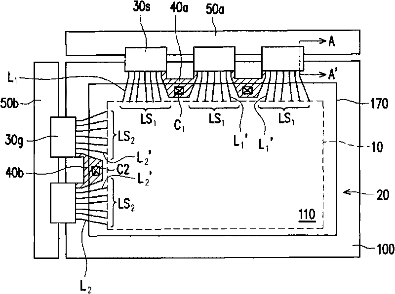
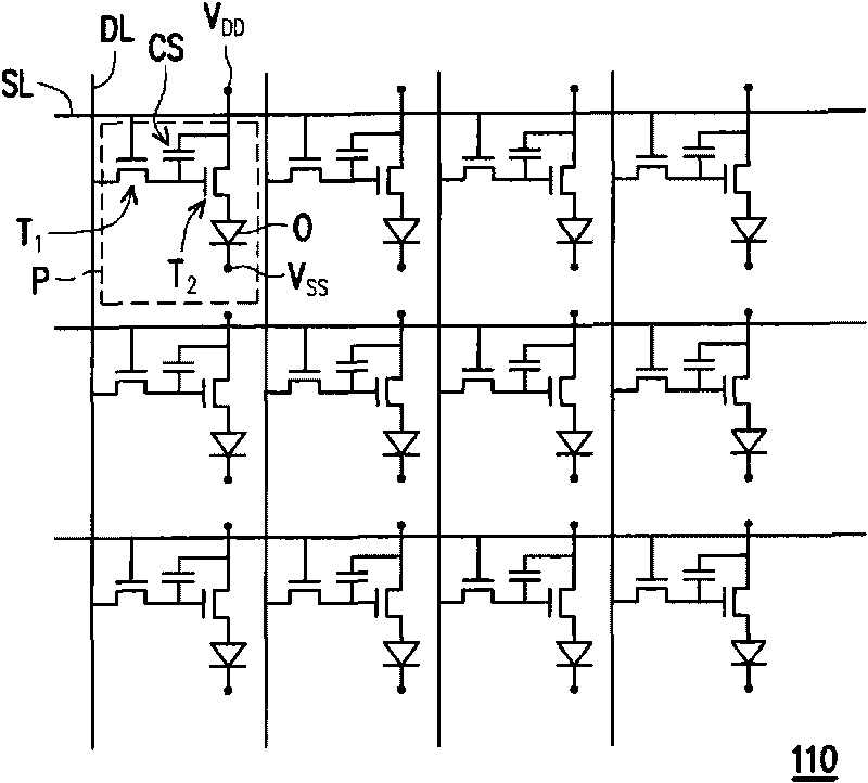
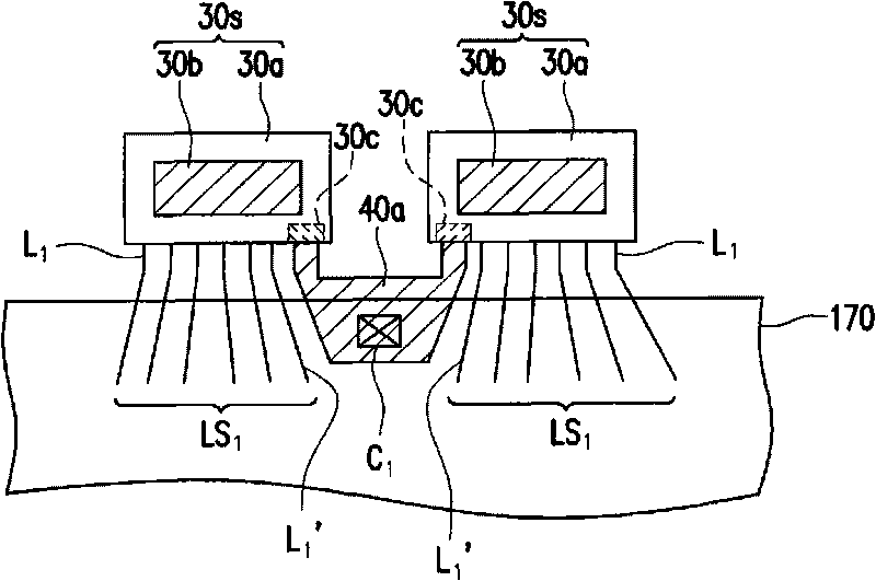
[0015] figure 1 It is a schematic top view of an electroluminescent device according to an embodiment of the invention. figure 2 Yes figure 1 The equivalent circuit diagram of the pixel array in the electroluminescent device. image 3 Yes figure 1 A partial schematic diagram of the peripheral circuit area. Figure 4 Yes figure 2 A schematic cross-sectional view of one of the pixel structures of the pixel array.

[0016] Please refer first figure 1 The electroluminescent device of this embodiment includes a substrate 100, a pixel array 110, a plurality of lead groups LS, a plurality of driving devices 30s, 30g, and at least one power transmission pattern 40a, 40b.

[0017] The substrate 100 has a display area 10 and a peripheral circuit area 20 located around the di...


PUM


Abstract

An electroluminescent device comprises a substrate, a pixel array, a plurality of lead groups, a plurality of driving devices and at least one power supply transmission pattern, wherein the substrate comprises a display area and a peripheral circuit area arranged on the periphery of the display area; the pixel array is arranged in the display area of the substrate and provided with a plurality of pixel structures, each pixel structure contains at least one active element and at least one light-emitting element which is electrically connected with the active element; the lead groups are arranged in the peripheral circuit area of the substrate and are electrically connected with the pixel array, wherein each lead group contains a plurality of leads; each driving device is electrically connected with one lead group; and the power supply transmission pattern is arranged in the peripheral circuit area of the substrate and positioned between adjacent two lead groups, wherein one end of the power supply transmission pattern is electrically connected with the light-emitting element of the pixel array and the other end of the power supply transmission pattern is electrically connected with the corresponding driving device.

Description

Technical field [0001] The present invention relates to a light emitting device, and in particular to an electroluminescent device. Background technique [0002] The electroluminescent device is a self-luminous (Emissive) device. Because the electroluminescent device has no viewing angle limitation, low manufacturing cost, high response speed (approximately more than a hundred times that of liquid crystal), power saving, DC drive that can be used in portable machines, large operating temperature range, light weight and easy Miniaturization and thinning of hardware equipment, etc. Therefore, electroluminescent devices have great development potential and are expected to become the next generation of novel flat-panel displays. [0003] Generally speaking, an electroluminescent device is composed of an upper electrode layer, a lower electrode layer, and a light-emitting layer sandwiched between the two electrode layers. The lower electrode layer is generally made of transparent cond...

Claims


Application Information

Patent Timeline
Patent Type & Authority Applications(China)
IPC IPC(8): H01L27/32H01L27/15H01L23/48H01L23/52G09F9/33
Inventor 柯凯元吴元均张立勋
Owner AU OPTRONICS CORP
Why Eureka
Try Eureka