Organic electroluminescence device for reducing patterning graphene electrodes based on laser and manufacturing method therefor

An electroluminescent device, a technology of graphene oxide, applied in the field of optoelectronics, can solve the problems of limiting the application of OLEDs, low brightness, and increasing the cost of OLED devices

Active Publication Date: 2012-08-22
中科精仪科技(广东)有限公司
View PDF5 Cites 15 Cited by
  • Summary
  • Abstract
  • Description
  • Claims
  • Application Information

AI Technical Summary

Problems solved by technology

Although LCD temporarily maintains its primary position in the display market, there are still some essential shortcomings: low brightness, slow response speed, non-active light source, etc., which prompts researchers to develop and explore new display devices
The traditional elect

Method used


Image

  • Organic electroluminescence device for reducing patterning graphene electrodes based on laser and manufacturing method therefor
  • Organic electroluminescence device for reducing patterning graphene electrodes based on laser and manufacturing method therefor
  • Organic electroluminescence device for reducing patterning graphene electrodes based on laser and manufacturing method therefor

Examples


Embodiment 1

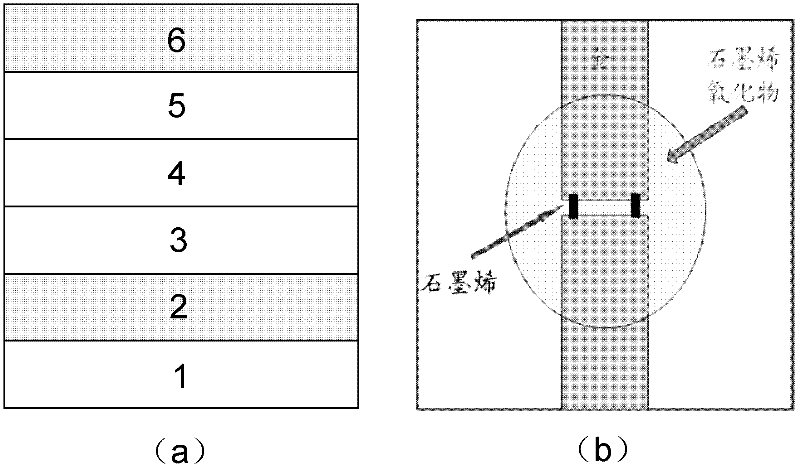
[0047] Fabrication of organic electroluminescent devices with ladder-shaped patterned graphene electrodes. The device structure is: Graphene (graphene, ~20nm) / m-MTDATA(30nm) / NPB(20nm) / Alq 3 (50nm) / LiF(1nm) / Al(100nm), such as figure 2 (a). Proceed as follows:

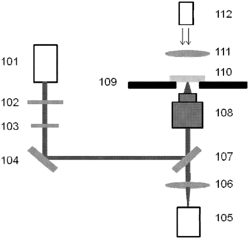
[0048] (1) On the cleaned substrate, a metal deposition system is used to grow a gold electrode as an extraction electrode, and the vacuum degree of the system is controlled at 1×10 during the growth process. -3 Pa, leave a channel with a width of about 90 μm in the middle of the gold electrode through the copper wire mask, the thickness of the gold electrode is 18 nm, the electrode length is 17 mm, and the width is 5 mm.

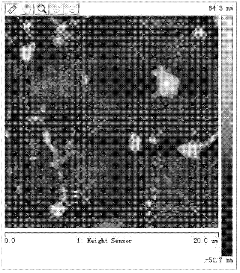
[0049] (2) Graphene oxide is spin-coated on the gold electrode, and the gold electrode and the channel in the middle are completely covered. The spin-coating speed is 1000rpm, and the spin-coating time is 18s. In a vacuum oven at 40°C, the film is Carry out drying treatment, the time is 60min.

...

Embodiment 2

[0058] Fabrication of organic electroluminescent devices with bow-tie patterned graphene electrodes. The device structure is: Graphene (graphene, ~20nm) / m-MTDATA(30nm) / NPB(20nm) / Alq 3 (50nm) / LiF(1nm) / Al(100nm), such as figure 2 (a).

[0059] On the cleaned substrate, a metal deposition system was used to grow a gold electrode as an extraction electrode, and the vacuum degree of the system was controlled at 1×10 during the growth process. -3Pa, a channel with a width of about 50 μm is left in the middle of the gold electrode through a copper wire mask, and the thickness of the gold electrode is 15 nm; then the graphene oxide is spin-coated on the gold electrode, and the gold electrode and its middle The channel is completely covered, the spin-coating speed is 1200rpm, the spin-coating time is 20s, and the film is dried in a vacuum oven at 40°C for 50min; then the graphene oxide is reduced by laser, and the process is the same as As described in Example 1, the selected laser...


PUM

PropertyMeasurementUnit
Thicknessaaaaaaaaaa
Average surface roughnessaaaaaaaaaa
Thicknessaaaaaaaaaa

Abstract

The invention belongs to the technical field of photoelectron and particularly relates to an organic electroluminescence device for reducing patterning graphene electrodes based on laser and a manufacturing method for the organic electroluminescence device. The organic electroluminescence device consists of a substrate, a gold electrode, the micron-dimension patterning graphene electrodes, an organic function layer and a cathode in sequence, wherein the gold electrode serves as an extraction electrode and is in a channel structure, the micron-dimension patterning graphene electrodes are lapped on the gold electrode at the two sides of each channel, and the micron-dimension patterning graphene electrodes are prepared by a laser write-through machining system capable of realizing laser point-by-point scanning. The obtained graphene electrodes are lower in the surface roughness and smoother in the surface, and therefore, the bottom-emission organic electroluminescence device prepared by the electrodes are higher in the degree of light-emitting homogeneity. The organic electroluminescence device and the manufacturing method break through the conventional concept for manufacturing the original large-area devices, the areas of the electrodes are reduced to the micron dimension, and patterns are led into the electrodes, so that the light-emitting area of the device is in a miniaturized pattern structure, thereby combining the organic electroluminescence device and the laser micro-nanomachining skillfully.

Description

technical field [0001] The invention belongs to the technical field of optoelectronics, and in particular relates to an organic electroluminescent device based on a laser reduction patterned graphene electrode and a preparation method thereof. technical background [0002] In recent years, the world's demand for information has grown rapidly, and the information industry has developed rapidly around the world. Information technology has become the cornerstone of today's economic activities and social life. Among them, as an important part of information technology - information display technology has played a key role in the acquisition of human knowledge and the improvement of life. [0003] As a new generation of display technology, flat panel display (FPD) has outstanding advantages such as light weight, small size, low power consumption, and no radiation, and has become the mainstream demand in the display field. Currently, FPDs mainly include liquid crystal displays (L...

Claims


Application Information

Patent Timeline
IPC IPC(8): H01L51/52H01L51/56C03C17/36
Inventor 孙洪波冯晶陈路
Owner 中科精仪科技(广东)有限公司
Why Eureka
Try Eureka