Light Emitting Device With Beveled Reflector And Manufacturing Method Of The Same

A light-emitting device and reflective structure technology, applied in the direction of semiconductor devices, electrical components, electric solid-state devices, etc., can solve the problems of multi-light energy, difficulty in applying small-sized light-emitting devices, loss, etc., and achieve the effect of increasing luminous efficiency

Inactive Publication Date: 2017-04-12
MAVEN OPTRONICS CO LTD
View PDF5 Cites 15 Cited by
  • Summary
  • Abstract
  • Description
  • Claims
  • Application Information

AI Technical Summary

Problems solved by technology

However, when the size of the light-emitting device is getting smaller and smaller, the solution that can be applied to a large size will become difficult to apply to a small-size light-emitting device.
[0004] In the current small-sized light-emitting device, due to the limitations of the existing technology, the reflective structure vertically covers the side of the fluorescent structure. This structure causes the light entering the reflective structure inside the fluorescent material to be larger due to the limitation of the critical angle. Part of it is reflected back into the fluorescent material or LED chip, and it is not easy to be guided to the top surface of the fluorescent structure to be extracted out of the light-emitting device, thus causing more light energy to be lost inside the light-emitting device, so its luminous efficiency can still be further improved
In addition, the current small-sized light-emitting devices do not have an effective solution for adjusting the light-emitting angle

Method used


Image

  • Light Emitting Device With Beveled Reflector And Manufacturing Method Of The Same
  • Light Emitting Device With Beveled Reflector And Manufacturing Method Of The Same
  • Light Emitting Device With Beveled Reflector And Manufacturing Method Of The Same

Examples


Embodiment Construction

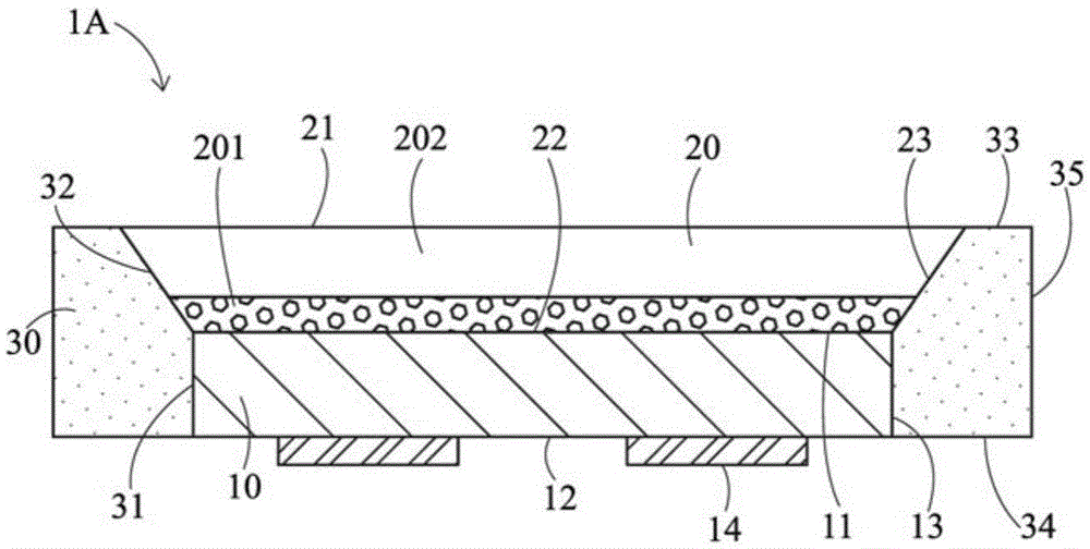
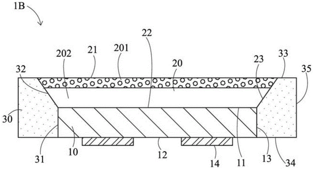
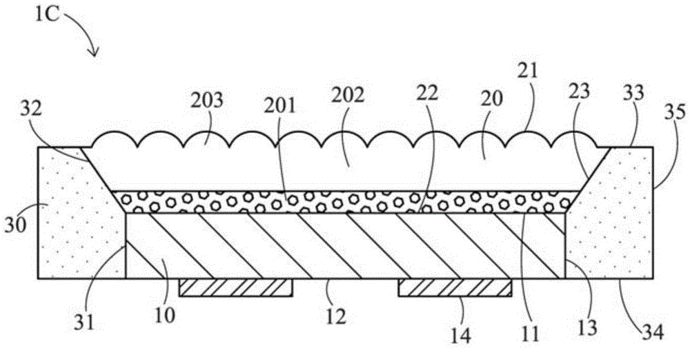
[0069] see figure 1 As shown, it is a schematic diagram of the light emitting device according to the first preferred embodiment of the present invention. The light emitting device 1A may include an LED chip 10 , a fluorescent structure 20 and a reflective structure 30 , and the technical content of the multiple components will be described in sequence as follows.

[0070] The LED chip 10 can be a flip-chip type chip, and can have an upper surface 11 , a lower surface 12 , a side surface 13 and an electrode group 14 in appearance. The upper surface 11 and the lower surface 12 are oppositely disposed, and the side surface 13 is formed between the upper surface 11 and the lower surface 12 and connects the upper surface 11 and the lower surface 12 . The electrode group 14 is disposed on the lower surface 12 and may have more than two electrodes. Electric energy (not shown in the figure) can be supplied into the LED chip 10 through the electrode group 14, and then the LED chip 1...


PUM


Abstract

The present invention provides a light emitting device with a beveled reflector and a manufacturing method of the same. The light emitting device includes an LED semiconductor die, a photoluminescent structure and a reflector. The photoluminescent structure is disposed on the LED semiconductor die, the side surface of the photoluminescent structure is beveled , and a lower surface of the photoluminescent structure adheres to an upper surface of the LED semiconductor die. The reflector wraps the side surface of the LED semiconductor die, and the side surface of the photoluminescent structure is beveled. A method to manufacture the above light emitting device is also disclosed. Advantages of this light emitting device with beveled reflector include increasing the light extraction efficiency, making the viewing angle tunable, improving spatial color uniformity and reducing the light source etendue realized in a compact form-factor size.

Description

technical field [0001] The present invention relates to a light emitting device and a manufacturing method thereof, in particular to a light emitting device with a corner reflective structure and a manufacturing method thereof. Background technique [0002] LED (Light Emitting Diode) chips are generally used to provide light sources for illumination or indication, and LED chips are usually placed in a package structure, or covered or covered by a fluorescent material to become a light emitting device. [0003] Light-emitting devices can obtain good luminous efficiency and specific luminous angles through appropriate design schemes. For example, the traditional high-economic-benefit bracket type (PLCC) LED package can increase its luminous efficiency through the design of the reflective cup and achieve a specific The light emitting angle, but the bracket type LED package has its inherent limitations, for example: the light travel path in the fluorescent glue is greatly differ...

Claims


Application Information

Patent Timeline
Patent Type & Authority Applications(China)
IPC IPC(8): H01L33/00H01L33/50H01L33/60
CPCH01L33/005H01L33/50H01L33/60H01L2933/0041H01L33/56H01L33/58H01L2924/12041H01L2933/0058
Inventor 陈杰王琮玺
Owner MAVEN OPTRONICS CO LTD
Why Eureka
Try Eureka