Power device and preparation method thereof

A technology for power devices and heat sinks, applied in the field of power devices and their preparation, can solve the problems of reducing the size of package interconnection, difficult to meet high-frequency and high-speed signal transmission, and difficult to realize high heat dissipation chips, etc., so as to improve the service life and reduce the temperature. Effect

Pending Publication Date: 2020-12-15
SHENNAN CIRCUITS
View PDF0 Cites 0 Cited by
  • Summary
  • Abstract
  • Description
  • Claims
  • Application Information

AI Technical Summary

Problems solved by technology

[0002] With the development of high-frequency and high-speed requirements for electronic products, traditional wire-bonded packaging and flip-chip packaging interconnection methods are difficult to meet the needs of high-frequency and high-speed signal transmission. Therefore, more and more chips are embedded in the substrate or fan-out at the wafer level. The process realizes bare chip packaging, reduces the package interconnection size and realizes the high-frequency and high-speed transmission of the chip to meet the signal integrity requirements
However, the embedded packaging scheme of the existing technology is difficult to meet the needs of high heat dissipation chips

Method used


Image

  • Power device and preparation method thereof
  • Power device and preparation method thereof
  • Power device and preparation method thereof

Examples


Embodiment Construction

[0014] The following will clearly and completely describe the technical solutions in the embodiments of the present application with reference to the accompanying drawings in the embodiments of the present application. Obviously, the described embodiments are only part of the embodiments of the present application, not all of them. Based on the embodiments in this application, all other embodiments obtained by persons of ordinary skill in the art without making creative efforts belong to the scope of protection of this application.

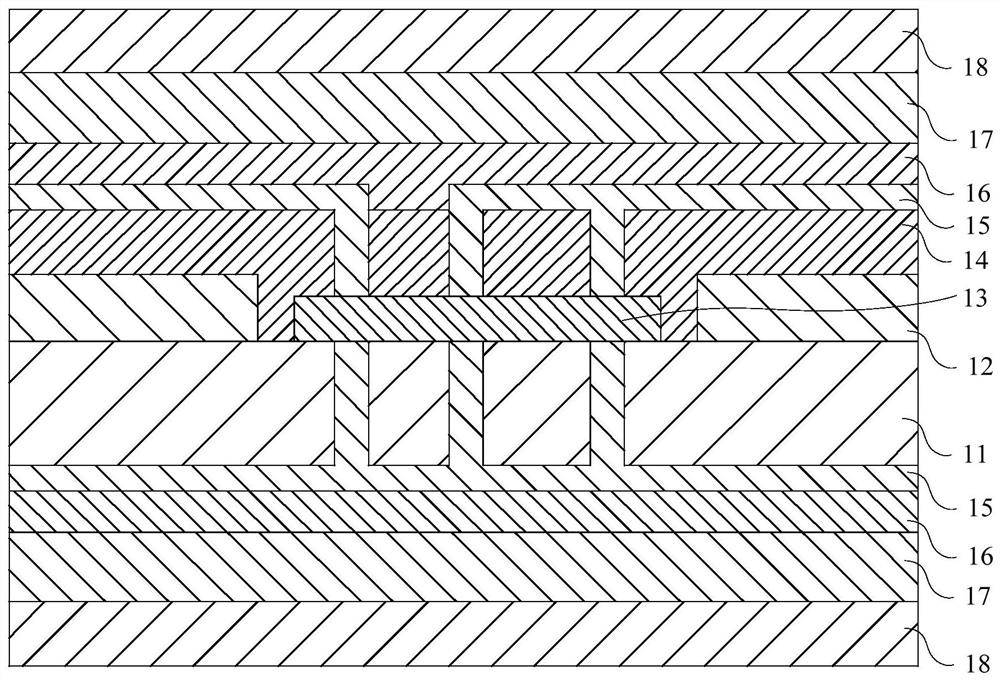
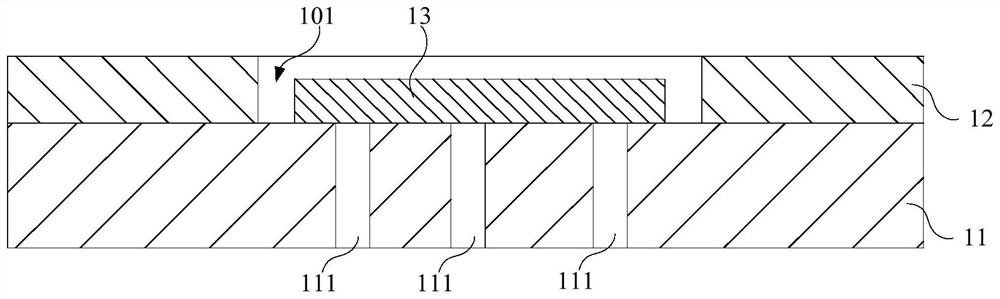
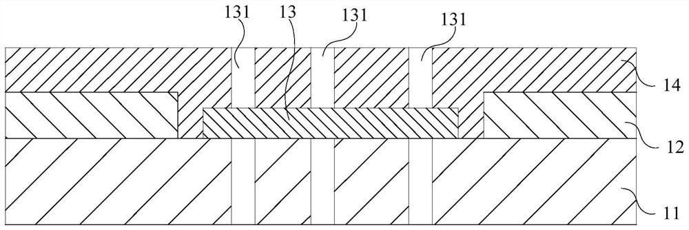
[0015] refer to figure 1 , figure 1 It is a schematic cross-sectional view of an embodiment of a power device provided in this application. The power device of this embodiment includes: a first insulating layer 11, a frame 12, a chip 13, a second insulating layer 14, two conductive pattern layers 15, two insulating and heat-conducting layer 16, two heat dissipation layers 17 and two heat sinks 18.

[0016] The first insulating layer 11 can be an...


PUM

PropertyMeasurementUnit
thicknessaaaaaaaaaa
thicknessaaaaaaaaaa

Abstract

The invention provides a power device. The power device comprises a first insulating layer, a frame which is arranged on one side of the first insulating layer and is provided with an accommodating space; a chip which is arranged in the accommodating space, and the first insulating layer is provided with a first via hole communicated with the chip; a second insulating layer which is arranged on one side, far away from the first insulating layer, of the frame, the accommodating space is filled with the second insulating layer to package the chip, and the second insulating layer is provided witha second via hole communicated with the chip; and two conductive pattern layers which are respectively arranged on one side, far away from the chip, of the first insulating layer and one side, far away from the first insulating layer, of the second insulating layer, and are respectively and electrically connected with the chip through the first via hole and the second via hole. According to the power device, double-sided heat dissipation of the chip can be realized, the temperature of the chip is reduced, and the service life of the chip is prolonged.

Description

technical field [0001] The present application relates to the technical field of chip packaging, in particular to a power device and a manufacturing method thereof. Background technique [0002] With the development of high-frequency and high-speed requirements for electronic products, traditional wire-bonded packaging and flip-chip packaging interconnection methods are difficult to meet the needs of high-frequency and high-speed signal transmission. Therefore, more and more chips are embedded in the substrate or fan-out at the wafer level. The process realizes bare chip packaging, reduces the package interconnection size and realizes the high-frequency and high-speed transmission of the chip to meet the signal integrity requirements. However, the embedded packaging solution in the prior art is difficult to meet the requirement of high heat dissipation chips. Contents of the invention [0003] The present application mainly provides a power device and a preparation method...

Claims


Application Information

Patent Timeline
Patent Type & Authority Applications(China)
IPC IPC(8): H01L23/367H01L21/50
CPCH01L21/50H01L23/367H01L2224/18
Inventor 黄立湘缪桦
Owner SHENNAN CIRCUITS
Why Eureka
Try Eureka