Packaging structure and packaging method of all-silicon carbide double-sided heat dissipation module

A packaging structure, silicon carbide technology, applied in the direction of semiconductor/solid-state device components, semiconductor devices, electrical components, etc., can solve the problems of dynamic unevenness, large parasitic inductance, low parasitic inductance, etc., to reduce dynamic unevenness, The effect of thermal performance improvement and stability improvement

Pending Publication Date: 2022-03-01
HUAZHONG UNIV OF SCI & TECH
View PDF0 Cites 0 Cited by
  • Summary
  • Abstract
  • Description
  • Claims
  • Application Information

AI Technical Summary

Problems solved by technology

[0005] Aiming at the defects of related technologies, the purpose of the present invention is to provide a novel double-sided heat dissipation packaging structure and packaging method with low parasitic inductance, low thermal resistance and relatively balanced parasitic parameters of each parallel power device circuit, aiming at solving the problem of existing silicon carbide Large parasitic inductance in the power package, unbalanced parasitic parameters between parallel power devices lead to dynamic unevenness, and poor heat dissipation of traditional modules

Method used


Image

  • Packaging structure and packaging method of all-silicon carbide double-sided heat dissipation module
  • Packaging structure and packaging method of all-silicon carbide double-sided heat dissipation module
  • Packaging structure and packaging method of all-silicon carbide double-sided heat dissipation module

Examples


Embodiment Construction

[0042] In order to make the object, technical solution and advantages of the present invention clearer, the present invention will be further described in detail below in conjunction with the accompanying drawings and embodiments. It should be understood that the specific embodiments described here are only used to explain the present invention, not to limit the present invention. In addition, the technical features involved in the various embodiments of the present invention described below can be combined with each other as long as they do not constitute a conflict with each other.

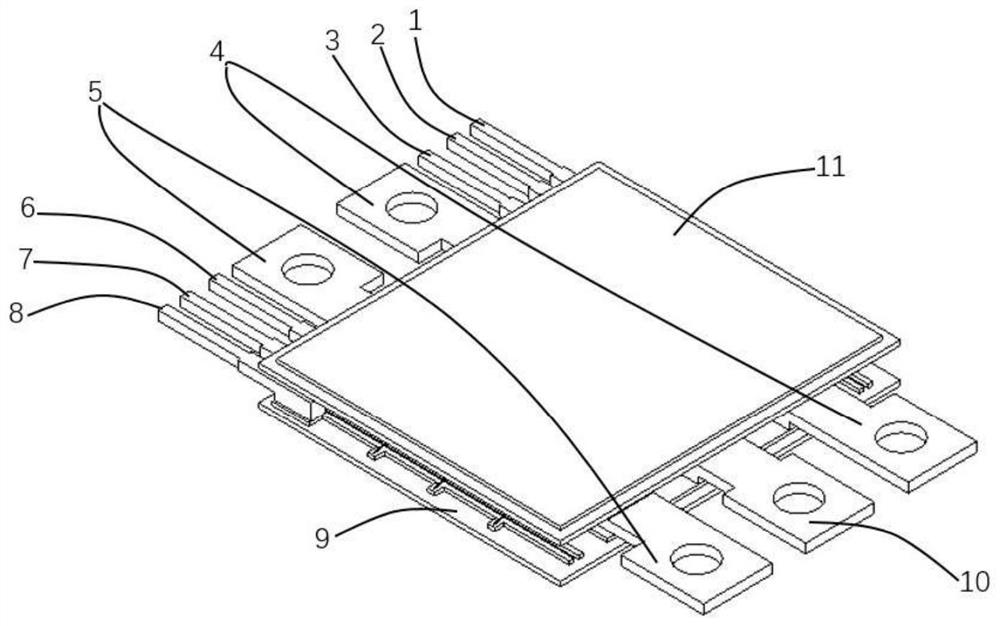
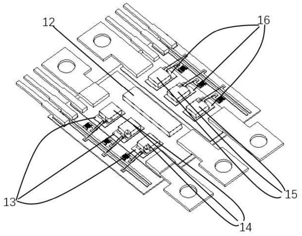
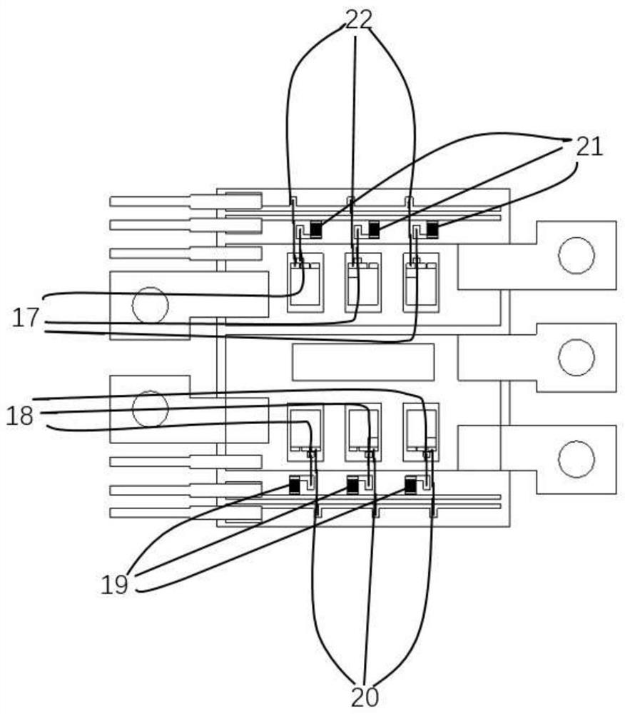
[0043] In order to achieve the above purpose, an embodiment of the present invention provides a full silicon carbide double-sided heat dissipation package structure, including a bottom DBC substrate, a silicon carbide power chip, a drive resistor, a pad, a top DBC substrate, a first heat sink and a second heat sink. heat sink;

[0044] The silicon carbide power chip and the drive resistor are d...


PUM

PropertyMeasurementUnit
melting pointaaaaaaaaaa

Abstract

The invention belongs to the technical field of packaging integration of power semiconductor modules, and discloses a packaging structure and a packaging method of a high-power all-silicon carbide module. The packaging structure comprises a bottom-layer direct copper-clad ceramic (DBC) substrate, a silicon carbide power chip (MOSFET), a driving resistor, a gasket, a top-layer DBC substrate and a connecting terminal, wherein the silicon carbide power chip (MOSFET) is mounted on the bottom-layer DBC substrate. A main power input terminal of the packaging structure adopts double-end outgoing lines, power leads have a structure with opposite current flow directions, parasitic inductance on part of power loops is counteracted by mutual inductance, and the parasitic inductance of a parallel chip commutation loop is more balanced; radiators can be assembled on the upper surface and the lower surface, so that two vertically parallel heat dissipation paths are provided for the power chip, and the heat resistance of the chip is reduced; the driving loop adopts a Kelvin structure, so that the influence of a common-source inductor on a driving signal is reduced, and the stability of the driving signal is enhanced. According to the packaging method, a reliable processing method is provided for the packaging structure, so that the packaging structure is realized.

Description

technical field [0001] The invention belongs to the technical field of packaging and integration of power semiconductor modules, and more specifically relates to a packaging structure of a full silicon carbide double-sided heat dissipation module and a packaging method thereof. Background technique [0002] The rapid iterative development of power electronic systems has higher requirements on the performance of power electronic devices. The performance of traditional Si devices has basically reached its physical limit. Therefore, it is urgent to develop new semiconductor material devices as substitutes. In order to further improve its switching characteristics and conduction characteristics, wide bandgap semiconductors (WBG) gradually come into people's field of vision. Under the same conditions, wide bandgap semiconductor material devices have higher breakdown voltage, higher conduction current, higher operating temperature, higher switching speed and lower switching loss t...

Claims


Application Information

Patent Timeline
Patent Type & Authority Applications(China)
IPC IPC(8): H01L25/07H01L25/00H01L23/367H01L23/482
CPCH01L25/071H01L25/50H01L23/3672H01L23/4822H01L2224/0603H01L2224/48091H01L2924/00014
Inventor 陈材鄢义洋黄志召刘新民康勇
Owner HUAZHONG UNIV OF SCI & TECH
Why Eureka
Try Eureka