Chip packaging body, manufacturing method thereof and electronic device

A chip packaging and electronic device technology, applied in semiconductor/solid-state device manufacturing, circuits, electrical components, etc., can solve the problems of excellent electrical and heat dissipation characteristics, the inability of chip packages to achieve, and achieve excellent low resistance characteristics and heat dissipation effects, Realize the effect of miniaturization, thinning, and simple structure

Pending Publication Date: 2021-03-26
SKY CHIP INTERCONNECTION TECH CO LTD
View PDF0 Cites 0 Cited by
  • Summary
  • Abstract
  • Description
  • Claims
  • Application Information

AI Technical Summary

Problems solved by technology

[0004] The present application provides a chip package and its manufacturing method and electronic device to solve the problem that the chip package in the prior art cannot realize the technical effects of miniaturization, thinning and excellent electrical and heat dissipation characteristics

Method used


Image

  • Chip packaging body, manufacturing method thereof and electronic device
  • Chip packaging body, manufacturing method thereof and electronic device
  • Chip packaging body, manufacturing method thereof and electronic device

Examples


Embodiment Construction

[0031] In order to make the technical problems solved by the present application, the adopted technical solutions and the achieved technical effects clearer, the technical solutions of the embodiments of the present application will be further described in detail below in conjunction with the accompanying drawings.

[0032] Reference herein to an "embodiment" means that a particular feature, structure, or characteristic described in connection with the embodiment can be included in at least one embodiment of the present application. The occurrences of this phrase in various places in the specification are not necessarily all referring to the same embodiment, nor are separate or alternative embodiments mutually exclusive of other embodiments. It is understood explicitly and implicitly by those skilled in the art that the embodiments described herein can be combined with other embodiments.

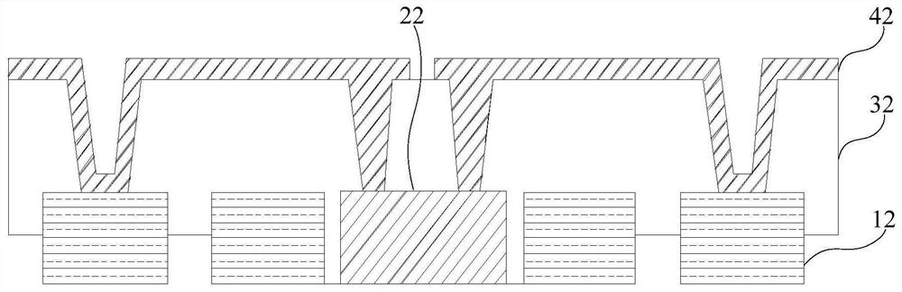
[0033] see figure 1 , figure 1 It is a structural schematic diagram of the first embod...


PUM


Abstract

The invention discloses a chip packaging body, a manufacturing method thereof and an electronic device, and the chip packaging body comprises a patterned metal substrate plate which is provided with afirst through hole; a chip arranged in the first through hole; a first insulating layer which covers the chip and the metal base material plate and fills the first through hole, wherein a second through hole is formed in the first insulating layer so as to expose part of the metal base material plate and the chip; patterned first conductive layers arranged on the first insulating layer and in thethrough hole, so that the chip is connected to the metal substrate through the first conductive layer. By means of the mode, the chip packaging body can achieve double-face heat dissipation of the chip, is simple in structure and short in electrical path and heat dissipation path, has the excellent low-resistance characteristic and heat dissipation effect, and miniaturization, lightness and thinness of the chip packaging body can be achieved.

Description

technical field [0001] The present application relates to the technical field of chip packaging, and in particular to a chip package, a manufacturing method thereof, and an electronic device. Background technique [0002] In recent years, with the Mosfet (Metal Oxide Semiconductor Field Effect Transistor, Metal-Oxide Semiconductor Field Effect Transistor, referred to as Metal Oxide Semiconductor Field Effect Transistor), IGBT (Insulated Gate Bipolar Transistor, Insulated Gate Bipolar Transistor) power modules are almost used in Among all power industrial products, the corresponding power devices are also steadily developing towards the direction of high performance, fast speed, small size and multi-chip connection packaging. [0003] However, the traditional wire bonding (semiconductor bonding gold wire) and double-sided copper interconnection technology and manufacturing methods are gradually difficult to meet the requirements of high performance, fast speed, small size, mu...

Claims


Application Information

Patent Timeline
Patent Type & Authority Applications(China)
IPC IPC(8): H01L23/31H01L23/495H01L23/48H01L21/56
CPCH01L23/49568H01L23/49541H01L23/481H01L23/3121H01L21/561H01L2224/18H01L2224/32257H01L2224/24245H01L2224/73267H01L2224/32245H01L2924/18162
Inventor 霍佳仁宋关强江京刘建辉
Owner SKY CHIP INTERCONNECTION TECH CO LTD
Why Eureka
Try Eureka