An embedded double-sided heat dissipation mosfet module package structure

A technology of double-sided heat dissipation and module packaging, which is applied in the direction of semiconductor/solid-state device parts, semiconductor devices, electrical components, etc., can solve the problems of low integration and large volume, so as to improve integration, solve technical problems, and improve heat dissipation effect of ability

Active Publication Date: 2022-07-08
合肥阿基米德电子科技有限公司
View PDF8 Cites 0 Cited by
  • Summary
  • Abstract
  • Description
  • Claims
  • Application Information

AI Technical Summary

Problems solved by technology

Each component of a typical power module is packaged discretely, with large volume and low integration level. It is necessary to optimize the packaging structure to achieve high heat dissipation performance and low energy consumption of the device.

Method used


Image

  • An embedded double-sided heat dissipation mosfet module package structure
  • An embedded double-sided heat dissipation mosfet module package structure
  • An embedded double-sided heat dissipation mosfet module package structure

Examples


Embodiment

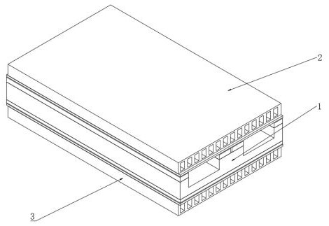
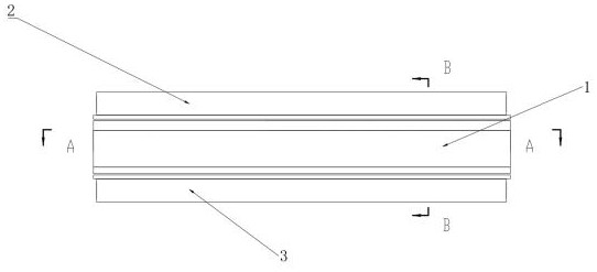
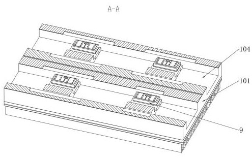
[0029] like Figures 1 to 9 As shown, an embedded double-sided heat dissipation MOSFET module packaging structure includes a DBC combination layer 1 and a MOSFET chip 9. The DBC combination layer 1 includes a DBC ceramic layer 101, and both sides of the upper surface of the DBC ceramic layer 101 are integrally provided with installation Intervals 104, square grooves 103 are respectively opened inside each installation interval 104, and MOSFET chips 9 are installed in each square groove 103 through the first copper sheet group 10 and the second copper sheet group 11, and the DBC composite layer 1 is up and down The surfaces are respectively mounted with an upper heat sink 2 and a lower heat sink 3 through a thermal interface material layer 6 . By embedding the MOSFET chip 9 in the DBC combination layer 1, the volume occupied by the MOSFET chip 9 is reduced, the overall integration of the module is improved, and the upper heat sink 2 and the lower heat sink 3 are respectively ar...


PUM


Abstract

The invention provides an embedded double-sided heat dissipation MOSFET module packaging structure, which relates to the technical field of power electronic power module packaging, and includes a DBC combination layer and a MOSFET chip. There are installation intervals, and square grooves are respectively opened inside each installation interval, and MOSFET chips are installed in each square groove through the first copper sheet group and the second copper sheet group. Through the packaging structure of the present invention, it is possible to The module integration is greatly improved, and the module volume is reduced by more than 40%. At the same time, the plane interconnection is realized, so that double-sided heat dissipation can be realized, and the heat dissipation capacity of the module is greatly improved, thus effectively solving the problem of the large volume caused by the discrete packaging of each component of a typical power module. , the integration is low, and the packaging structure needs to be reasonably designed and optimized to achieve high heat dissipation performance and low energy consumption of the device.

Description

technical field [0001] The invention relates to the technical field of power electronic power module packaging, in particular to an embedded double-sided heat dissipation MOSFET module packaging structure. Background technique [0002] As one of the core devices for energy conversion and transmission, high-power MOSFET devices are widely used in aerospace, electric vehicles, new energy, etc., power transmission fields; and with the evolution of the semiconductor industry, silicon carbide chips have been applied, and the chip junction temperature The demand for power modules with low power consumption and high efficiency continues to increase. Electronic packaging is usually composed of several semiconductor chips and different packaging materials, which provide mechanical support, electrical interconnection, insulation protection, foreign body, moisture protection, and heat dissipation paths for the device. Each component of a typical power module is packaged separately, wh...

Claims


Application Information

Patent Timeline
Patent Type & Authority Patents(China)
IPC IPC(8): H01L23/367H01L23/46H01L23/492H01L25/07
CPCH01L23/367H01L23/46H01L24/40H01L25/072H01L2224/40137
Inventor 宋一凡马坤孙亚萌周洋刘胜
Owner 合肥阿基米德电子科技有限公司
Why Eureka
Try Eureka