Pixel unit array, sensor chip and electronic device

A pixel unit and array technology, applied in the direction of circuits, electrical components, electric solid-state devices, etc., can solve problems affecting the autofocus performance of image sensors

Pending Publication Date: 2020-12-18
SHENZHEN GOODIX TECH CO LTD
View PDF0 Cites 0 Cited by
  • Summary
  • Abstract
  • Description
  • Claims
  • Application Information

AI Technical Summary

Problems solved by technology

[0003] In an image sensor using PDAF autofocus technology, a pixel structure in which two adjacent pixels share a microlens (2×1OCL for short) can be used. In this pixel structure, the photosensitive unit in the pixel unit used for autofocus phase detection Prone to photoelectron saturation, affecting the autofocus performance of the image sensor

Method used


Image

  • Pixel unit array, sensor chip and electronic device
  • Pixel unit array, sensor chip and electronic device
  • Pixel unit array, sensor chip and electronic device

Examples


Embodiment Construction

[0036] In order to make the purpose, technical solution and advantages of the present application clearer, the embodiments of the present application will be further described in detail below in conjunction with the accompanying drawings and the embodiments. It should be understood that the specific embodiments described here are only used to explain the present application, and are not intended to limit the present application.

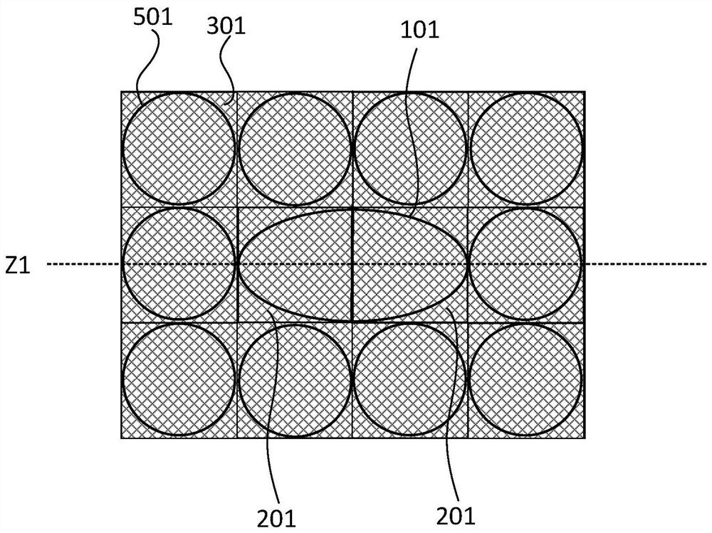
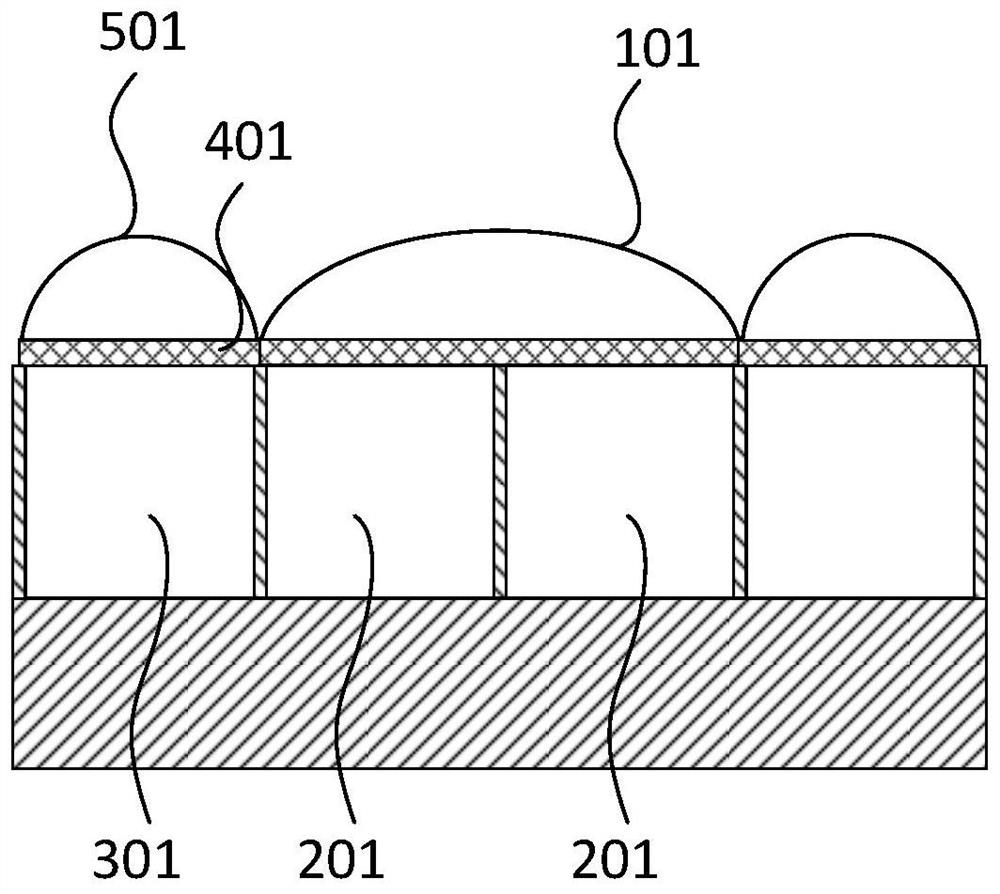
[0037] In the PDAF autofocus technology, known implementation methods include: shielding pixels, dividing an original pixel into two sub-pixels, sharing a microlens (On Chip Lens, OCL for short) between two adjacent pixels, and sharing a microlens (OCL for short) with four adjacent pixels. microlenses. Please refer to figure 1 and figure 2, is a known pixel structure in which two adjacent pixels share a microlens (2×1 OCL for short) in an image sensor, that is, a microlens OCL101 is arranged on two adjacent pixel units 201 for phase detection The...


PUM


Abstract

The embodiment of the invention provides a pixel unit array and electronic equipment. In the pixel unit array, first pixel units and second pixel units are arranged on a substrate layer, the substratelayer comprises a plurality of pixel areas arranged in an array, each first pixel unit occupies one pixel area, and each second pixel unit occupies M rows and N columns of pixel areas in the array formed by the plurality of pixel areas; wherein M and N are both positive integers, M + N is greater than or equal to 4, and the volume of the sub-pixel is greater than that of the first pixel unit; theshading layers are used for shading incident light, each shading layer comprises two sub shading layers with the same shape, and the sub shading layers are in one-to-one correspondence with the sub pixels; each sub-shading layer is arranged on the corresponding sub-pixel and covers part of the photosensitive area of the corresponding sub-pixel; the two sub-shading layers are symmetrical about thereference plane mirror image, and the reference plane is the plane where the contact surface of the two sub-pixels is located. According to the invention, the focusing performance of the pixel unit array under strong light is improved.

Description

technical field [0001] The embodiments of the present application relate to the technical field of semiconductors, and in particular to a pixel unit array, a sensor chip, and an electronic device. Background technique [0002] In electronic products represented by mobile phones, autofocus during shooting is one of its very important functions, which improves the quality of captured images and the user's camera experience. Currently, commonly used autofocus technologies include Phase Detection Auto Focus (PDAF for short), Contrast Detection Auto Focus (CDAF for short), and the like. [0003] In an image sensor using PDAF autofocus technology, a pixel structure in which two adjacent pixels share a microlens (2×1OCL for short) can be used. In this pixel structure, the photosensitive unit in the pixel unit used for autofocus phase detection It is prone to the problem of photoelectron saturation, which affects the autofocus performance of the image sensor. Contents of the inve...

Claims


Application Information

Patent Timeline
IPC IPC(8): H01L27/146
CPCH01L27/14605H01L27/14623H01L27/14627H01L27/14645
Inventor 兰洋沈健姚国峰袁晓龙
Owner SHENZHEN GOODIX TECH CO LTD
Why Eureka
Try Eureka