Contact-type image sensor

An image sensor and contact technology, applied in the field of image sensors, can solve problems affecting image recognition, large dark voltage, and inability to receive light signals

Pending Publication Date: 2020-12-25
WEIHAI HUALING OPTO ELECTRONICS CO LTD
View PDF0 Cites 1 Cited by
  • Summary
  • Abstract
  • Description
  • Claims
  • Application Information

AI Technical Summary

Problems solved by technology

[0006] From the above, the photosensitive output and dark voltage of each row are different and random, resulting in the inability to correct the image sensor, which will seriously affect the sensitivity of the photoelectric conversion chip, the dynamic range and the output variation of each row, affecting image recognition; extreme cases If the speed of transmitting the object to be detected is too slow and the line cycle is too long, the dark voltage will be too large, and the dark voltage will reach the limit value, which will make the photoelectric conversion chip in a saturated state and cannot receive light signals at all; therefore, it is urgent to develop a new contact image sensor

Method used


Image

  • Contact-type image sensor
  • Contact-type image sensor
  • Contact-type image sensor

Examples


Embodiment Construction

[0026] In order to make the purpose, technical solutions and advantages of the embodiments of the present invention clearer, the technical solutions in the embodiments of the present invention will be clearly and completely described below in conjunction with the drawings in the embodiments of the present invention. Obviously, the described embodiments It is a part of the embodiments of the present invention, rather than all embodiments; based on the embodiments of the present invention, all other embodiments obtained by those of ordinary skill in the art without creative work, all belong to the protection scope of the present invention .

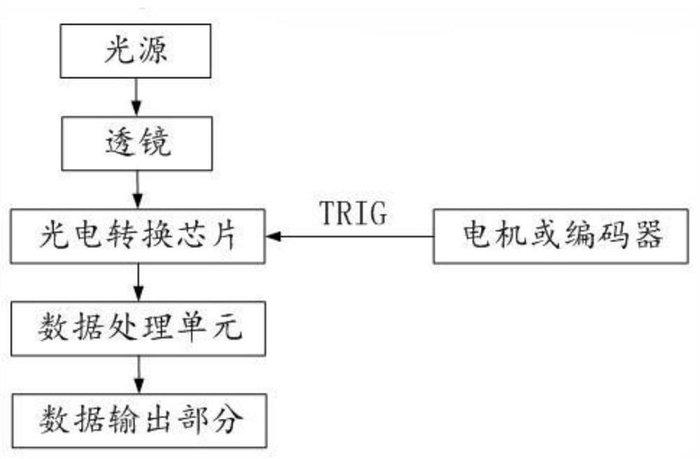
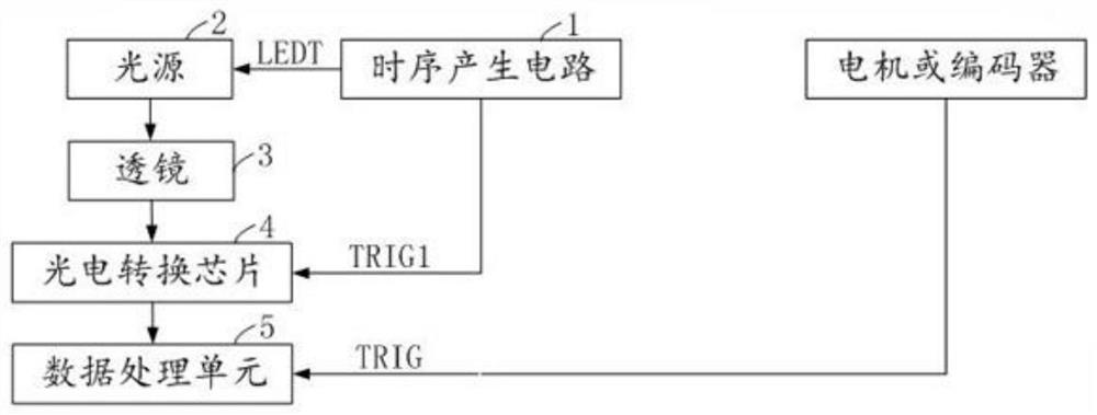
[0027] image 3 A schematic structural diagram of a contact image sensor provided in Embodiment 1 of the present invention, as shown in image 3 As shown, a contact image sensor, the contact image sensor has a preset scanning surface, and the scanning surface is used to correspond to the surface to be scanned of the original, and the conta...


PUM


Abstract

The invention discloses a contact-type image sensor. The contact-type image sensor is provided with a preset scanning surface corresponding to a to-be-scanned surface of a manuscript. The contact-typeimage sensor comprises a time sequence generation circuit which is used for generating a light source control signal LRDT and a line scanning control signal TRIG1; a light source which is used for irradiating the manuscript; a lens which is used for collecting the reflected light emitted by the light source and reflected by the manuscript and emitting the reflected light to a photoelectric conversion chip; the photoelectric conversion chip which is used for converting the received optical signal into an electric signal; and a data processing unit which is used for receiving and processing theelectric signal output by the photoelectric conversion chip according to a trigger pulse TRIG sent by an encoder for transmitting an object to be detected. The photosensitive signals output by the photoelectric conversion chip are the same, so that the output stability, the dynamic range and the sensitivity of the image sensor are guaranteed.

Description

technical field [0001] The invention belongs to the technical field of image sensors, and in particular relates to a contact image sensor. Background technique [0002] In the prior art, the block diagram of the existing contact image sensor is as follows: figure 1 As shown, it is composed of a light source, a lens, a photoelectric conversion chip, a data processing unit, and a data output part. Image sensor scanning In order to match the moving speed of the external object to be detected, the trigger pulse TRIG is sent by the motor or encoder that transmits the object to be detected, and the light emitted by the light source shines on the original, and the image, text, etc. on the original generate reflected light or transmitted light The reflected light or transmitted light passes through the lens and irradiates the photoelectric conversion chip. The photoelectric conversion chip converts the received optical signal into an electrical signal, and after being processed by ...

Claims


Application Information

Patent Timeline
IPC IPC(8): H04N1/031
CPCH04N1/0318H04N1/02815H04N1/031H04N2201/0081
Inventor 姜利韩晓伟林永辉戴朋飞
Owner WEIHAI HUALING OPTO ELECTRONICS CO LTD
Why Eureka
Try Eureka