Embedded touch display device

A touch display device and embedded technology, applied in the direction of instrument, electrical digital data processing, data processing input/output process, etc., can solve problems affecting product use experience, etc., and achieve the effect of ensuring user experience and avoiding compression.

Pending Publication Date: 2021-01-05
HONG FU JIN PRECISION IND (SHENZHEN) CO LTD +1
View PDF12 Cites 3 Cited by
  • Summary
  • Abstract
  • Description
  • Claims
  • Application Information

AI Technical Summary

Problems solved by technology

When the conductivity of the backlight module is poor, the induced negative charges will gradually accumulate on the side of the backlight module close to the touch electrodes, and generate electrostatic attraction between the positive charges accumulated on the touch electrodes, and the electrostatic attraction will compress The air gap between the backlight module and the touch panel forms a denser air wave. When the electrostatic attraction decreases or becomes zero, a thinner air wave is formed between the air gap. When the denser air wave and the thinner When air waves are alternately generated, sound waves are formed. If the frequency of the sound waves is at a frequency that can be heard by the human ear, it can be heard by the human ear, which will affect the user experience of the product

Method used


Image

  • Embedded touch display device
  • Embedded touch display device
  • Embedded touch display device

Examples


Embodiment 1

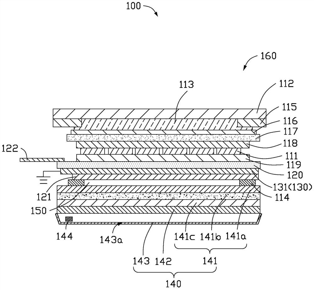
[0023] like figure 1 As shown, the in-cell touch display device 100 provided in Embodiment 1 includes a display panel 160 and a backlight module 140 stacked on top of each other. The backlight module 140 provides the display panel 160 with the backlight required for displaying images. on the light output path of the backlight module 140 . The display panel 160 is used for displaying images.

[0024] The display panel 160 is provided with a plurality of touch electrodes 111, and the in-cell touch display device 100 further includes a grounded inductive charge elimination element 130, and the inductive charge elimination element 130 is disposed on a side of the backlight module 140 close to the display panel 160, It is used to eliminate the induced charge in the backlight module 140 due to the induction with the charge on the touch electrode 111 . In this embodiment, the inductive charge elimination element 130 is a conductive anti-static layer (Anti-Static Layer, ASL) 131 , a...

Embodiment 2

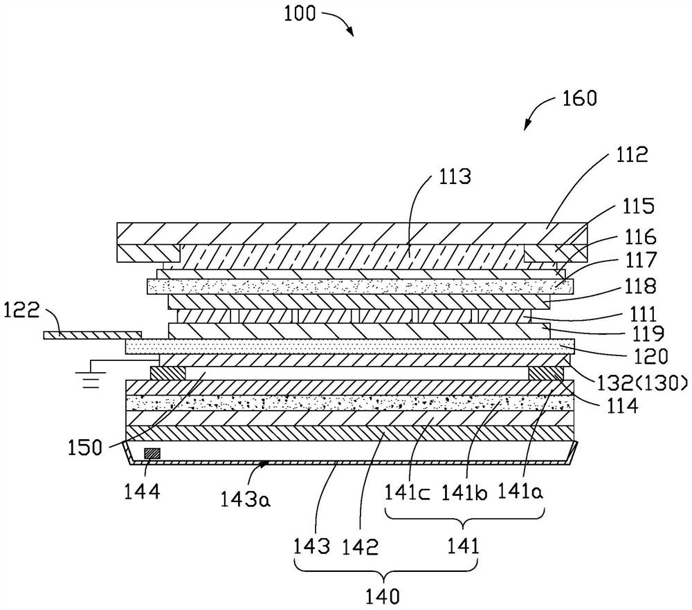
[0034] The main difference between the embedded touch display device 100 provided in the second embodiment and the first embodiment is that: image 3 As shown, the in-cell touch display device 100 is not additionally provided with an antistatic layer 131 for eliminating static charges, but uses a lower polarizer 132 as an inductive charge elimination component 130 , and the lower polarizer 132 is conductive. The lower polarizer 132 is arranged on the side of the thin film transistor array substrate 120 close to the backlight module 140. In this embodiment, the lower polarizer 132 is arranged between the thin film transistor array substrate 120 and the backlight module 140, and the touch electrodes 111 are arranged on the thin film transistor array substrate 120 and the backlight module 140. The side of the transistor array substrate 120 away from the lower polarizer 132 . The surface resistance of the lower polarizer 132 is less than 10 10 ohm / sq, for example 10 7 ohm / sq or ...

Embodiment 3

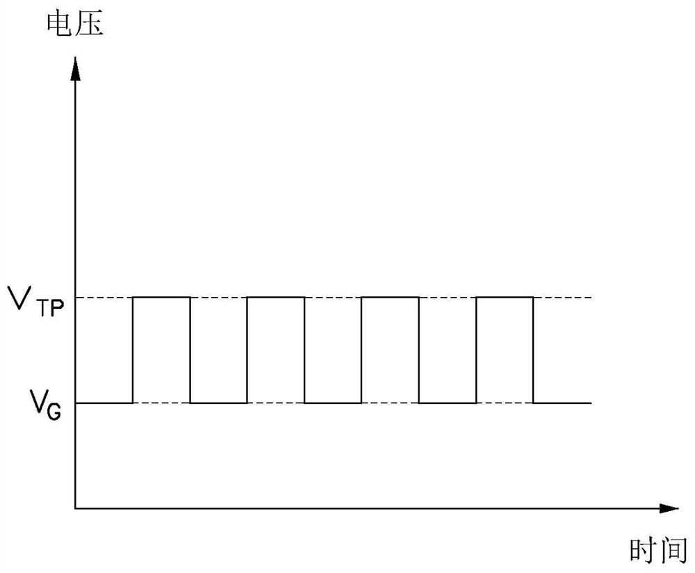
[0036] The main difference between the embedded touch display device 100 provided in the third embodiment and the first embodiment is that: Figure 4 As shown, the in-cell touch display device 100 of the present invention is not equipped with an induced charge elimination element, but by adjusting the driving signal of the driving element 133 electrically connected to the touch electrode 111, thereby avoiding the induction charge in the backlight module 140 . The driving element 133 is used for sending a driving signal to the touch electrode 111 , wherein the driving signal is an alternating positive and negative voltage signal.

[0037] like Figure 5 As shown, a driving cycle t 0 Include a drive signal adjacent to a positive voltage signal (eg, Figure 5 The voltage value in V TP A high level signal) and a negative voltage signal (such as, Figure 5 The voltage value in the -V TP The time corresponding to the low level signal), a driving cycle t 0 Also includes zero p...


PUM


Abstract

The invention provides an embedded touch control display device which comprises a display panel and a backlight module which are arranged in a mutually stacked mode, wherein the display panel is arranged on a light emitting path of the backlight module, a plurality of touch control electrodes are arranged in the display panel, and the embedded touch control display device further comprises a grounded inductive charge eliminating element; the grounded inductive charge eliminating element is arranged on one side, close to the display panel, of the backlight module and used for eliminating induced charges generated by induction of the touch electrode in the backlight module. According to the embedded touch display device provided by the invention, inductive charges generated by induction withthe touch electrodes in the backlight module are eliminated through positive and negative alternating voltage signals emitted by the inductive charge eliminating element and the driving element; therefore, compression of an air gap between the embedded touch display device and the backlight module due to electrostatic attraction between the touch electrodes and the backlight module is avoided, noise caused by compression of the air gap is avoided, and the use experience of a product is guaranteed.

Description

technical field [0001] The present invention relates to the field of touch display, in particular to an embedded touch display device. Background technique [0002] In the prior art, a positive voltage signal (the voltage signal changes alternately between zero potential and positive voltage) is applied to the touch electrodes of an in-cell touch panel to sense a conductive object (for example, a finger ) and the capacitance change between the touch electrode, if the capacitance changes, it can be determined that the finger touches the touch panel. When a positive voltage signal acts on the touch electrodes, the touch electrodes may accumulate a large amount of positive charges, and the side of the backlight module close to the touch electrodes is affected by the positive charges of the touch electrodes to generate induced negative charges. When the conductivity of the backlight module is poor, the induced negative charges will gradually accumulate on the side of the backli...

Claims


Application Information

Patent Timeline
Patent Type & Authority Applications(China)
IPC IPC(8): G06F3/044G06F3/041
CPCG06F3/044G06F3/0418G06F3/0412G06F3/04166G06F3/047
Inventor 翁裕复黄鸿运
Owner HONG FU JIN PRECISION IND (SHENZHEN) CO LTD
Why Eureka
Try Eureka