Supercharge Your Innovation With Domain-Expert AI Agents!

Method for forming multi-wafer stacking structure

A technology of stacking structure and wafers, applied in electrical components, semiconductor/solid-state device manufacturing, circuits, etc., can solve problems such as the inability to meet the needs of multi-wafer bonding and trimming

Pending Publication Date: 2021-01-05
WUHAN XINXIN SEMICON MFG CO LTD
View PDF6 Cites 0 Cited by
  • Summary
  • Abstract
  • Description
  • Claims
  • Application Information

AI Technical Summary

Problems solved by technology

Whether in terms of economic cost or process difficulty, the traditional trimming process cannot meet the trimming requirements of multi-wafer bonding

Method used


Image

  • Method for forming multi-wafer stacking structure
  • Method for forming multi-wafer stacking structure
  • Method for forming multi-wafer stacking structure

Examples


Embodiment 1

[0084] Combine below figure 2 , Figure 3a-3d as well as Figure 4a ~ 4f A method for forming a multi-wafer stack structure provided by an embodiment of the present invention is described in detail.

[0085] The multi-wafer stacking structure of this embodiment includes a carrier wafer 110 and two wafers stacked on the carrier wafer 110 in sequence.

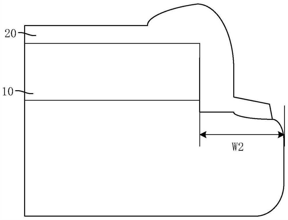
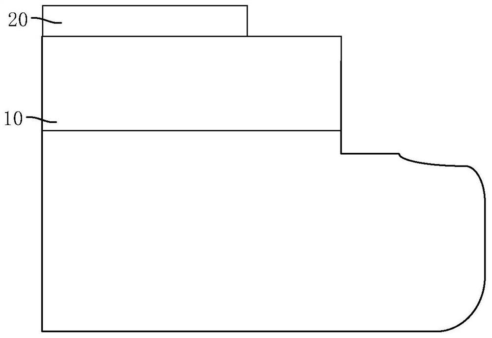
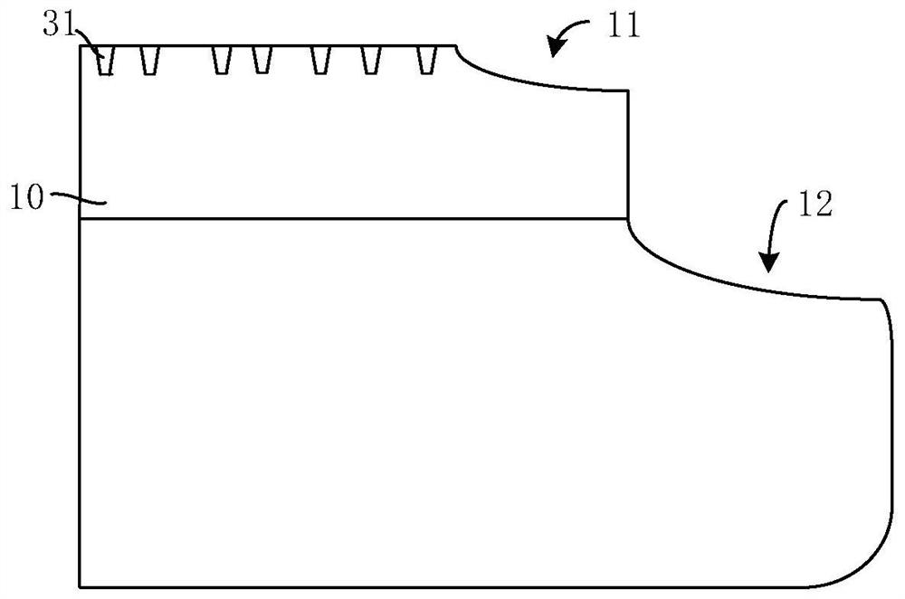
[0086] Figure 3a It is a schematic cross-sectional structure diagram of the first stack structure provided in this embodiment. like Figure 3a As shown, step S1 is first performed to bond the first wafer 120 whose front edge area has been trimmed to the carrier wafer 110, and then grind and thin the first wafer 120 from the back side 120b of the first wafer 120. circle 120, to reserve part of the thickness of the first wafer 120, and form a first stack structure 100, the first stack structure is in the shape of a boss,

[0087] Wherein, the first stack structure 100 has an edge gap area M1 at the edge of the bonding surf...

Embodiment 2

[0110] Compared with Embodiment 1, the multi-wafer stacking structure of this embodiment includes a carrier wafer 110 and N wafers sequentially stacked on the carrier wafer 110 , where N≥3, and N is a positive integer. And after the second stack structure in step S3 is formed, then step S42 is performed to form the (i-1)th bonding hole on the front surface of the (i-1)th stack structure, and ) bonding holes are filled with the (i-1)th metal layer, the (i-1)th metal layer also covers the front side of the (i-1)th stack structure, and then the (i-1)th trimming the edge area of ​​the front side of the stack structure to remove the edge gap area of ​​the (i-1)th stack structure, and then planarizing the (i-1)th metal layer to form the (i-1)th bond fit pad.

[0111] Then step S5 is performed, bonding the i-th wafer whose front edge area has been trimmed to the (i-1) stacked structure, and then grinding and thinning the i-th wafer from the back side of the i-th wafer circle, to re...


PUM


Abstract

According to the method of forming the multi-wafer stacking structure provided by the invention, the trimming process after the previous bonding is pushed to the bonding hole before the subsequent bonding is filled with the metal layer, so that the edge gap area caused by the previous bonding is reduced; possible bad areas formed between the metal layers filled in the bonding holes after the previous bonding and before the subsequent bonding are not on the same plane, and projection parts of the edge gap areas and the possible bad areas are overlapped, so that the trimming width of the trimming process after pushing can be reduced; therefore, the effective area of the multi-wafer stacking structure is increased, possible bad areas are removed, and bad areas (copper rings are prevented frombeing formed in the forming process of the bonding pad) are avoided.

Description

technical field [0001] The invention belongs to the technical field of integrated circuit manufacturing, and in particular relates to a method for forming a multi-wafer stack structure. Background technique [0002] In some existing semiconductor processes, such as 3D-IC wafer bonding and subsequent wafer thinning processes, in order to ensure the integrity and smoothness of the wafer edge, the wafer needs to be trimmed (Trim). [0003] Before bonding two adjacent wafers, one of the wafers needs to be trimmed for the first time, and then the two adjacent wafers are bonded, and one of the wafers is first ground and thinned. Then use acid etching combined with the second trimming process to obtain the ideal edge. [0004] In the multi-wafer stacking process, the previous steps are repeated, because each subsequent added wafer needs to have a complete support at the bottom, otherwise the edges of the adjacent two wafers are easily broken during the grinding process, therefore,...

Claims


Application Information

Patent Timeline
Patent Type & Authority Applications(China)
IPC IPC(8): H01L21/18H01L21/02
CPCH01L21/187H01L21/02035H01L21/02021H01L21/02016H01L21/02008
Inventor 叶国梁
Owner WUHAN XINXIN SEMICON MFG CO LTD
Features
  • R&D
  • Intellectual Property
  • Life Sciences
  • Materials
  • Tech Scout
  • Unparalleled Data Quality
  • Higher Quality Content
  • 60% Fewer Hallucinations
Learn More