Supercharge Your Innovation With Domain-Expert AI Agents!

Multi-wafer stack trimming method

A wafer and trimming technology, which is applied in the manufacturing of electrical components, circuits, semiconductor/solid-state devices, etc., and can solve problems such as the inability to meet the needs of multi-wafer bonding and trimming.

Active Publication Date: 2021-04-23
WUHAN XINXIN SEMICON MFG CO LTD
View PDF5 Cites 0 Cited by
  • Summary
  • Abstract
  • Description
  • Claims
  • Application Information

AI Technical Summary

Problems solved by technology

Whether in terms of economic cost or process difficulty, the traditional trimming process cannot meet the trimming requirements of multi-wafer bonding

Method used


Image

  • Multi-wafer stack trimming method
  • Multi-wafer stack trimming method
  • Multi-wafer stack trimming method

Examples


Embodiment 2

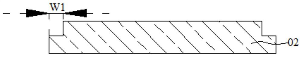
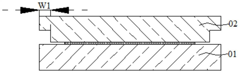
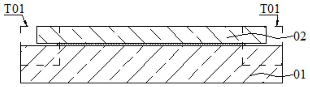
[0082] In the subsequent step S4 of processing each wafer in the second embodiment, it is all satisfied that the edge region of the i-th wafer whose back surface is thinned is trimmed, and the trimming width is different in the lateral direction (perpendicular to the thickness direction). Greater than the edge trimming width W of the second wafer after backside thinning D2 , that is, when 2≤i≤N, W Di ≤W D2 . In this way, the trimming in all wafer processing processes in the second embodiment is limited to W. D2 In the range.

[0083] In the second embodiment, by filling the top filling layer, the wafer trimming is controlled to a smaller range than that in the first embodiment. Exemplarily, using the multi-wafer stacking trimming method of the first embodiment can control the wafer trimming width to within 10 mm, and using the multi-wafer stacking trimming method of the second embodiment can control the wafer trimming width to 5 mm within. Embodiment 2 Controlling wafer ...


PUM


Abstract

The present invention provides a multi-wafer stacking and trimming method. After cutting the edge of the i-th wafer, bonding with the i-1th wafer and thinning it, the edge area of ​​the stacked i-th wafer is trimmed to form Wafers with good edges are stacked; the underfill layer is filled afterwards; the existence of the underfill layer makes the defects generated on the edge of the adjacent subsequent wafer bonded to the stacked i-piece wafer move outward, so that the adjacent subsequent wafer The trimming width is set to be small, and provides support for adjacent subsequent wafers when bonding and thinning, so as not to split during thinning; The edge trimming width of the thinned second wafer can remove the defects generated by the thinned edge after the subsequent wafer adjacent to the i-th wafer is bonded to the stacked i-th wafer. W di ≤W d2 , all wafer processing trimming is limited to W d2 Within the range, reduce the trimming width of the wafer and increase the effective area of ​​the wafer.

Description

technical field [0001] The invention belongs to the technical field of integrated circuit manufacturing, and in particular relates to a multi-wafer stack trimming method. Background technique [0002] In some existing semiconductor processes, such as 3D-IC wafer bonding and subsequent wafer thinning processes, in order to ensure the integrity and smoothness of the wafer edge, the wafer needs to be trimmed. [0003] Before bonding two adjacent wafers, one of the wafers needs to be trimmed for the first time, and then the two adjacent wafers are bonded. The top wafer is first ground and thinned, and then acid is applied. Etching is combined with a second trimming process to achieve the desired edge. [0004] In the multi-wafer stacking process, the previous steps are repeated. Since each subsequent wafer grinding process on the top layer needs to have complete support at the bottom, otherwise the edge of the grinding process will be broken. Trimming is required, and the widt...

Claims


Application Information

Patent Timeline
Patent Type & Authority Patents(China)
IPC IPC(8): H01L21/67H01L21/60H01L21/50
CPCH01L21/50H01L21/67121H01L2021/60007
Inventor 叶国梁刘天建
Owner WUHAN XINXIN SEMICON MFG CO LTD
Features
  • R&D
  • Intellectual Property
  • Life Sciences
  • Materials
  • Tech Scout
  • Unparalleled Data Quality
  • Higher Quality Content
  • 60% Fewer Hallucinations
Learn More