Capacitor array, preparation method thereof and storage device

A capacitor array and capacitor technology, applied in capacitors, circuits, electrical components, etc., can solve the problem of increasing the contact area between the belt-shaped fixed layer and the lower electrode, so as to improve the resistance to high-temperature treatment and liquid surface tension ability, low preparation cost, and stable performance

Pending Publication Date: 2021-01-05
CHANGXIN MEMORY TECH INC
View PDF0 Cites 3 Cited by
  • Summary
  • Abstract
  • Description
  • Claims
  • Application Information

AI Technical Summary

Problems solved by technology

However, limited by etching and other processes, it is difficult to increase the contact area between the strip-shaped pinned layer and the bottom electrode by increasing the thickness of the strip-shaped pinned layer.

Method used


Image

  • Capacitor array, preparation method thereof and storage device
  • Capacitor array, preparation method thereof and storage device
  • Capacitor array, preparation method thereof and storage device

Examples


Embodiment Construction

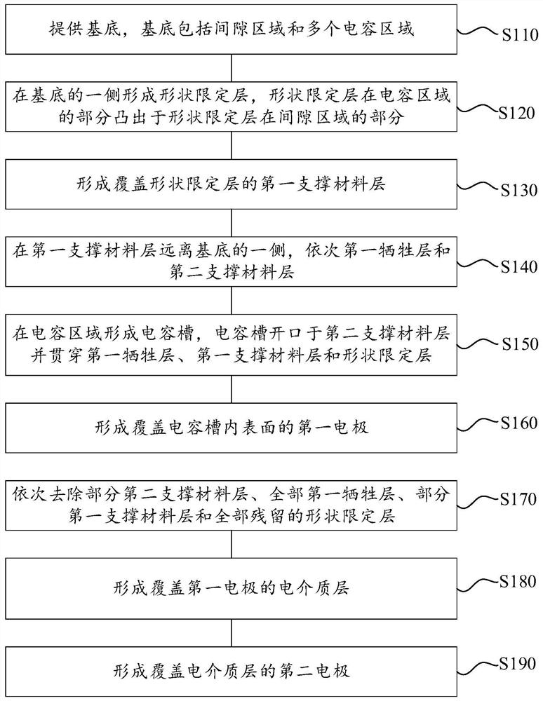
[0093]Example embodiments will now be described more fully with reference to the accompanying drawings. However, the example embodiments can be implemented in various forms, and should not be construed as being limited to the examples set forth herein; on the contrary, the provision of these embodiments makes the present disclosure more comprehensive and complete, and fully conveys the concept of the example embodiments To those skilled in the art. The described features, structures or characteristics may be combined in one or more embodiments in any suitable manner. In the following description, many specific details are provided to give a sufficient understanding of the embodiments of the present disclosure.

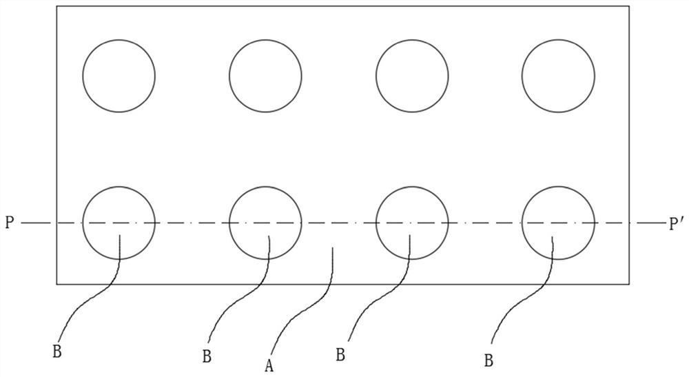
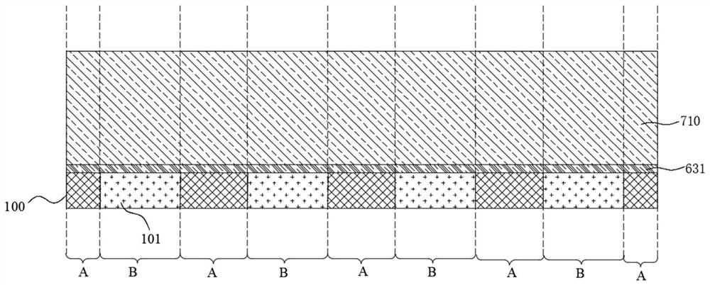
[0094]In the figure, the thickness of regions and layers may be exaggerated for clarity. The same reference numerals in the figures indicate the same or similar structures, and thus their detailed descriptions will be omitted.

[0095]When a structure is “on” another structure, it...


PUM

PropertyMeasurementUnit
thicknessaaaaaaaaaa
thicknessaaaaaaaaaa
thicknessaaaaaaaaaa

Abstract

The invention provides a capacitor array, a preparation method thereof and a storage device, and belongs to the technical field of semiconductors. The preparation method of the capacitor array comprises the following steps: providing a substrate comprising a gap region and a plurality of capacitor regions; forming shape defining layers on one side of the substrate, wherein a part of the shape defining layers in the capacitor regions protrude out of a part of the shape defining layers in the gap region; forming a first support material layer covering the shape defining layer; sequentially forming first sacrificial layers and a second support material layer; forming capacitor grooves in the capacitor regions, wherein the capacitor grooves penetrate through the first sacrificial layers, the first support material layer and the shape defining layers; forming first electrodes covering the inner surfaces of the capacitor grooves; sequentially removing part of the second support material layers, all the first sacrificial layers, part of the first support material layer and all the residual shape limiting layers; forming dielectric layers covering the first electrodes; forming second electrode layer covering the dielectric layers. The preparation method of the capacitor array can improve the stability of the capacitor array.

Description

Technical field[0001]The present disclosure relates to the field of semiconductor technology, and in particular to a capacitor array, a manufacturing method thereof, and a storage device.Background technique[0002]In order to increase the capacitance of the columnar capacitor, the columnar capacitor often increases the height of the lower electrode to enlarge the contact area between the lower electrode and the dielectric layer, so that the columnar capacitor has a high aspect ratio. At the same time, a strip-shaped fixed layer can be provided in the middle of the lower electrode to improve the stability of the columnar capacitor.[0003]As the aspect ratio of the columnar capacitor continues to increase, it is necessary to increase the contact area between the strip-shaped fixed layer and the lower electrode, otherwise the lower electrode is easily damaged due to insufficient contact area. However, due to the limitation of processes such as etching, it is difficult to increase the con...

Claims


Application Information

Patent Timeline
Patent Type & Authority Applications(China)
IPC IPC(8): H01L21/70H01L21/84H01L27/01H01L27/108H01L27/11H01L27/13H01L49/02
CPCH01L27/016H01L27/13H01L21/707H01L21/84H01L28/40H10B12/30H10B10/00
Inventor 徐正弘
Owner CHANGXIN MEMORY TECH INC
Why Eureka
Try Eureka