Double-channel airtight packaging structure of flip-chip and process of double-channel airtight packaging structure

A packaging structure and airtight technology, applied in electrical components, electrical solid devices, circuits, etc., can solve the problems of large thermal resistance, small chip contact area, poor heat dissipation efficiency, etc., to reduce the overall thermal resistance and shorten the working time , the effect of improving work efficiency

Inactive Publication Date: 2021-01-05
XIAN MICROELECTRONICS TECH INST
View PDF10 Cites 1 Cited by
  • Summary
  • Abstract
  • Description
  • Claims
  • Application Information

AI Technical Summary

Problems solved by technology

[0005] The object of the present invention is to overcome the disadvantages of poor heat dissipation efficiency due to small chip contact area and large thermal resistance when the airtight packaging s

Method used


Image

  • Double-channel airtight packaging structure of flip-chip and process of double-channel airtight packaging structure
  • Double-channel airtight packaging structure of flip-chip and process of double-channel airtight packaging structure
  • Double-channel airtight packaging structure of flip-chip and process of double-channel airtight packaging structure

Examples


Embodiment 1

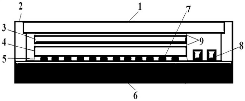
[0039] Such as figure 1 As shown, the double-channel hermetic packaging structure includes a cover plate 1, a casing 6 and a sealing ring 2 installed on the casing 6, and a flip chip 4 and a heat sink 3 are installed in the sealing ring 2 , the cover plate 1 is installed on the top of the heat sink 3, the heat sink 3 is installed on the top of the flip chip 4, and the flip chip 4 is installed on the top of the shell 6, and the heat sink 3 is connected with the cover plate 1 and the flip chip A heat dissipation layer is arranged between the 4.

[0040] Concrete preparation process is as follows:

[0041] S1: first install the sealing ring 2 on the casing 6, temporarily fix the cover plate 1 on the upper part of the sealing ring 2, and fix the flip chip 4 on the top of the casing 6;

[0042] S2: According to the vertical height difference between the upper surface of the flip chip 4 and the bottom surface of the cover plate 1, prepare the heat sink 3 according to the vertical ...

Embodiment 2

[0047] Prepare the cavity packaging structure, prepare a stepped sealing ring 2 on the shell 6, both the cover plate 1 and the sealing ring are made of nickel-plated Kovar material, and the fit gap between the cover plate 1 and the sealing ring 2 is ≤0.1 mm, the surface height difference is less than or equal to 0.5mm, and a flip chip 4 with a size of 20mm×20mm is welded inside the tube shell 6 . Package according to the following steps:

[0048] (1) Using optical equipment to measure the vertical height difference between the upper surface of the flip-chip 4 and the step on the sealing ring 2 where the cover plate 1 is pre-placed;

[0049] (2) Prepare an AlN ceramic sheet whose thickness is determined according to the measured value of the vertical height difference between the upper surface of the flip-chip 4 and the step of the sealing ring 2, which is 50 μm-200 μm smaller than the above-mentioned vertical height difference;

[0050] (3) Cut the AlN ceramic chip into a hea...

Embodiment 3

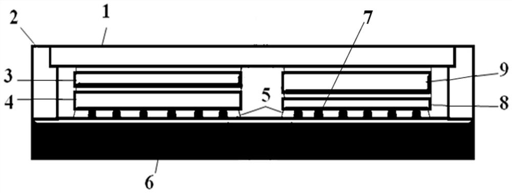
[0060] When processing two chips at the same time, if the thickness of the two chips is inconsistent, such as figure 2 As shown, the cavity packaging structure is prepared. A stepped gold-plated aluminum alloy sealing ring 2 is prepared on the shell 6. The cover plate 1 is made of an aluminum alloy with excellent mechanical properties and thermal conductivity, and the surface is plated with gold. The cover plate The matching clearance and surface height difference between 1 and sealing ring 2 meet the requirements, and there are two flip-chip bare chips with dimensions of 15mm×18mm and 10mm×15mm respectively welded in the cavity. Package according to the following steps:

[0061] (1) Using optical equipment to measure the height difference between the upper surface of the two flip-chips 4 and the steps of the sealing ring 2;

[0062] (2) Prepare an Al-SiC sheet heat sink 3, the thickness of which is determined according to the measured value of the height difference between ...


PUM

PropertyMeasurementUnit
Thicknessaaaaaaaaaa

Abstract

The invention discloses a double-channel airtight packaging structure of a flip-chip and a process thereof, and belongs to the field of electronic packaging. The flip-chip is installed on the tube shell, the heat sink is installed above the flip-chip, the cover plate is installed above the heat sink, the cover plate, the sealing welding ring and the tube shell are welded at the joint to form a closed cavity, and the problem that the service life of a device is short due to the fact that the flip-chip is packaged in a non-airtight mode can be solved. Meanwhile, airtight packaging is carried outon the cover plate with the large thickness in a laser fusion sealing mode, large deformation of the cover plate under mechanical or thermal stress can be effectively avoided, and therefore the stress borne by the flip chip is reduced, and cracking of flip welding spots is prevented. The airtight packaging structure is provided with the upper heat dissipation channel and the lower heat dissipation channel, and compared with a single heat dissipation channel only passing through convex points, the overall heat resistance can be reduced by multiple times when double channels of the heat sink above the chip and the cover plate are increased for heat dissipation.

Description

technical field [0001] The invention belongs to the field of electronic packaging, and relates to a dual-channel hermetic packaging structure of a flip chip and a technology thereof. Background technique [0002] Flip-chip welding technology implements wiring and array I / O arrangement on the entire active surface of the chip, and uses flip-chip welding technology to interconnect the substrate or the shell directly through the micro-bumps on the chip surface. One of the key technologies for density assembly and miniaturization and multi-function of electronic devices. For flip-chip chips, especially chips with high power consumption and high heat generation such as large-scale I / O processors, having a good heat dissipation channel is one of the key factors to ensure long-term work of flip-chip chips. [0003] At present, the heat dissipation package of flip-chip bare chips is usually a non-hermetic package, and the fluid air on the back of the flip-chip promotes the dissipat...

Claims


Application Information

Patent Timeline
IPC IPC(8): H01L23/367H01L23/373H01L23/10H01L21/52
CPCH01L21/52H01L23/10H01L23/367H01L23/3737H01L2224/73204H01L2224/73253
Inventor 汤姝莉赵国良张健薛亚慧
Owner XIAN MICROELECTRONICS TECH INST
Why Eureka
Try Eureka