
Logic resource evaluation method

A logic resource and resource technology, applied in the field of logic resource evaluation, can solve problems such as inability to complete wiring, inability to quickly predict the number of hardware resources, inability to complete technology mapping, etc.

Active Publication Date: 2021-01-15
S2C
View PDF2 Cites 0 Cited by
  • Summary
  • Abstract
  • Description
  • Claims
  • Application Information

AI Technical Summary

Problems solved by technology

When the problem of insufficient on-chip resources occurs, the designer needs to modify the RTL description and perform time-consuming design synthesis process iterations
[0004]Because the design synthesis process includes multiple steps, when the designer writes and modifies the RTL description, he cannot quickly predict the amount of on-chip hardware resources required for the circuit to be implemented on the FPGA. This can result in technology mapping not being done or routing not being done and resulting in multiple design iterations

Method used


Image

  • Logic resource evaluation method
  • Logic resource evaluation method

Examples


Embodiment Construction

[0030] The present invention will be described in further detail below in conjunction with specific examples, but the embodiments of the present invention are not limited thereto.

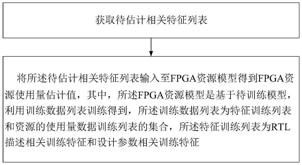
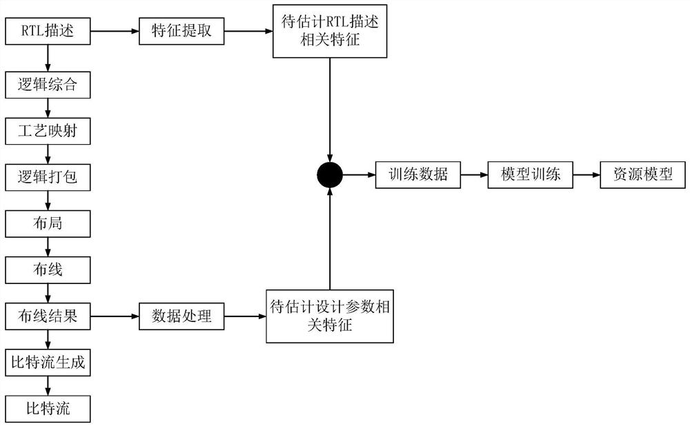
[0031] See figure 1 and figure 2 , figure 1 is a flow chart of a logic resource evaluation method provided by an embodiment of the present invention, figure 2 It is a flow chart of another logical resource evaluation method provided by the embodiment of the present invention. A logical resource assessment method comprising:

[0032] Step 1. Obtain a list of related features to be estimated.

[0033] Specifically, in this embodiment, a list of related features to be estimated needs to be acquired before performing the machine learning-based RTL-level FPGA resource usage estimation.

[0034] Further, step 1 also includes:

[0035] Step 1.1. Obtain the related features of the RTL description to be estimated and the related features of the design parameters to be estimated respectively.

[003...


PUM


Abstract

The invention discloses a logic resource evaluation method. The method comprises the steps of obtaining a to-be-estimated related feature list; inputting the to-be-estimated related feature list intoan FPGA resource model to obtain an FPGA resource usage amount estimated value, the FPGA resource model being obtained by training by using a training data list based on a to-be-trained model, the training data list being a set of a feature training list and a resource usage amount data training list, and the feature training list being a set of RTL description related training features and designparameter related training features. According to the FPGA resource model obtained through the method, the on-chip resource usage amount needed by RTL description can be rapidly obtained at the initial stage of design, the estimability of design and logic synthesis is enhanced, and the number of iterations is reduced.

Description

technical field [0001] The invention belongs to the technical field of semiconductors, and in particular relates to a logic resource evaluation method. Background technique [0002] Field Programmable Gate Array (Field Programmable Gate Array, FPGA) is an important semiconductor device, which can realize the logic design required by users through on-site reprogramming. When the designer uses the hardware description language to program the register transfer level (RTL) of the circuit, the RTL description will be converted into bit stream data for configuring the internal structure of the FPGA through multiple design synthesis steps. These design synthesis steps include Logic synthesis, technology mapping, logic packaging, place and route, and more. [0003] At this stage, for a given RTL description, the number of FPGA on-chip hardware resources required by it generally requires the completion of logic packaging and routing before the full number of resources can be obtaine...

Claims


Application Information

Patent Timeline
Patent Type & Authority Applications(China)
IPC IPC(8): G06F30/398G06F30/343G06F17/18
CPCG06F30/398G06F30/343G06F17/18Y02D10/00
Inventor 林铠鹏祁仲冬李伟
Owner S2C
Learn More