Semiconductor structure and forming method thereof

A technology of semiconductor and segment structure, applied in semiconductor devices, semiconductor/solid-state device manufacturing, electric solid-state devices, etc., can solve problems such as missing segments, and achieve the effect of improving accuracy and enhancing protection.

Pending Publication Date: 2021-01-19
SEMICON MFG INT (SHANGHAI) CORP +1
View PDF0 Cites 0 Cited by
  • Summary
  • Abstract
  • Description
  • Claims
  • Application Information

AI Technical Summary

Problems solved by technology

[0003] In the process of forming a semiconductor structure, block cuts are usually used to form more compact patterns at the 10nm technology node. However, after the block cut is formed, the subsequent etching process will cause a certain amount of etching on the block cut. rate, eventually leading to missing segments

Method used


Image

  • Semiconductor structure and forming method thereof
  • Semiconductor structure and forming method thereof
  • Semiconductor structure and forming method thereof

Examples


Embodiment Construction

[0031] As mentioned in the background, the precision of the pattern formed by the semiconductor structure in the prior art is poor.

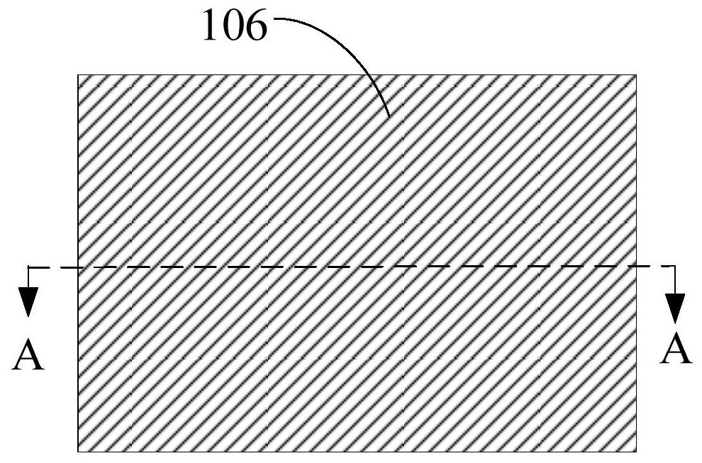
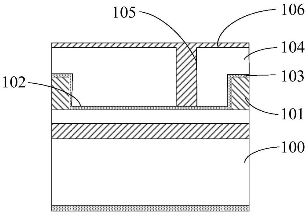
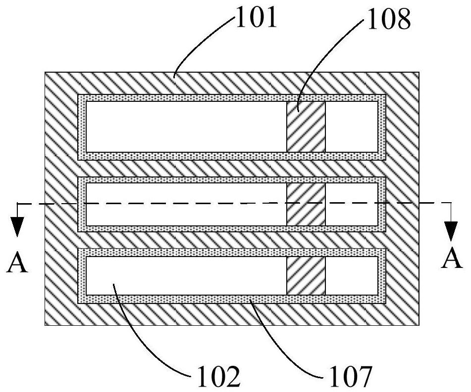
[0032] Please refer to Figure 1 to Figure 2 , figure 2 Yes figure 1 A schematic cross-sectional view along the A-A line provides a layer to be etched 100; a core layer 101 is formed on the layer to be etched 100, and a first trench 102 is provided in the core layer 101, and the first trench 102 is formed along the first trench 102. Extending in one direction, a sidewall layer 103 is formed on the top surface of the core layer 101 and the sidewall and bottom surface of the first trench 102; a sacrificial layer 104 is formed on the sidewall layer 103, and the sacrificial The layer 104 has a split opening 105 exposing the first trench 102 , and a split segment layer 106 is formed in the split opening 105 , and the split segment layer 106 fills the split opening 105 .

[0033] After forming the segment layer 106, planarize the sacrificial laye...


PUM

PropertyMeasurementUnit
thicknessaaaaaaaaaa
thicknessaaaaaaaaaa

Abstract

The invention discloses a semiconductor structure and a forming method thereof. The semiconductor structure comprises a to-be-etched layer; a core layer which is located on the layer to be etched, wherein a first groove is formed in the core layer, and the first groove extends in the first direction; a segmentation section structure which is located in the first groove, wherein the segmentation section structure penetrates through the first groove in the second direction, the second direction is different from the first direction, and the segmentation section structure comprises a second segmentation layer and first segmentation layers located on the side wall and the bottom surface of the second segmentation layer; a side wall which is positioned on the surface of the side wall of the first groove. The second segmentation layer is protected through the first segmentation layer, so that the second segmentation section is prevented from being lost in a subsequent etching process, and the accuracy of forming a graph in the semiconductor structure is improved.

Description

technical field [0001] The invention relates to the technical field of semiconductor manufacturing, in particular to a semiconductor structure and a forming method thereof. Background technique [0002] In the semiconductor integrated circuit manufacturing process, a semiconductor structure is formed on a semiconductor substrate through a series of procedures, such as deposition, photolithography, etching, and the like. Among them, the photolithography process is to form a desired pattern in the photoresist, obtain a patterned photoresist, and define a region to be etched. The etching process is used to transfer the pattern in the patterned photoresist to the layer to be etched. [0003] In the process of forming a semiconductor structure, block cuts are usually used to form more compact patterns at the 10nm technology node. However, after the block cut is formed, the subsequent etching process will cause a certain amount of etching on the block cut. rate, eventually leadi...

Claims


Application Information

Patent Timeline
Patent Type & Authority Applications(China)
IPC IPC(8): H01L21/78H01L21/683
CPCH01L21/78H01L21/6835H01L2221/68327H01L21/0337H01L21/0338H01L21/0335H01L21/0332
Inventor 汤霞梅施维窦涛苏波胡友存
Owner SEMICON MFG INT (SHANGHAI) CORP
Why Eureka
Try Eureka