Chemical supply system for manufacturing semiconductor and purification method thereof

A technology for supplying systems and chemicals, applied in the pipeline system, gas/liquid distribution and storage, mechanical equipment, etc., can solve the problems of unreasonable pipeline cleaning methods, time-consuming and labor-intensive, etc., to save time, reduce risks, reduce The effect of labor costs

Inactive Publication Date: 2021-01-29
JIANGSU YAKE FREE SEMICON TECH CO LTD
View PDF5 Cites 1 Cited by
  • Summary
  • Abstract
  • Description
  • Claims
  • Application Information

AI Technical Summary

Problems solved by technology

[0010] Purpose of the invention: The purpose of the present invention is to solve the problem that the existing semiconductor supply system pipeline cleaning method is unreasonable, time-consuming and labor-intensive

Method used


Image

  • Chemical supply system for manufacturing semiconductor and purification method thereof

Examples


Embodiment 1

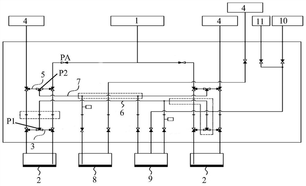
[0039] like figure 1 As shown, a chemical supply system for manufacturing semiconductors includes at least two identical sets of supply equipment and a deposition chamber 1 connected to the liquid outlet of each supply equipment chemical tank, and each set of supply equipment includes a For the chemical tank 2 that stores chemicals that need to be deposited, there is a first bridging pipe 3 between the air inlet and the liquid outlet of the chemical tank 2, and a first three-way valve P1 is set on the first bridging pipe 3, The third port of the first three-way valve P1 is connected to the corresponding port of the first three-way valve P1 at the first bridge pipe 3 of another chemical tank 2, and the air inlet of the chemical tank 2 is connected to the supercharger 4 through a pipeline , the pipeline from the chemical tank 2 to the supercharger 4 and the pipeline from the chemical tank 2 to the deposition chamber 1 are provided with a second bridging pipe 5, and the third of ...

Embodiment 2

[0048] A method of purifying a chemical supply system for the manufacture of semiconductors comprising the steps of:

[0049] 1) When the remaining amount of medicine in one chemical tank 2 is insufficient, open the path that another set of chemical tank 2 is transported to the deposition chamber 1, and at the same time, the current set of supply equipment passes through the first branch 6 or the second branch 7 Transport the medicine to the bridging pipe of another set of supply equipment, and open the bridge pipe to transport the tee in the direction of the deposition chamber 1, so that the medicine in the chemical tank 2 of the current supply equipment can be completely used up;

[0050] 2) When the medicine in the chemical tank 2 of the current set of supply equipment is completely used up, close all directions of the first three-way valve P1 and the second three-way valve P2 of the other set of supply equipment, and open the booster connected to the solvent tank 8 device ...


PUM


Abstract

The invention discloses a chemical supply system for manufacturing a semiconductor. The chemical supply system comprises at least two sets of identical supply equipment and a deposition cavity connected with a liquid outlet of a chemical tank of each set of supply equipment, wherein each set of supply equipment comprises a chemical tank for storing a chemical to be deposited; a first bridging pipeis arranged between an air inlet and a liquid outlet of the chemical tank; a first three-way valve is arranged on the first bridging pipe; a third interface of the three-way valve is connected with acorresponding interface of the first three-way valve at the first bridging pipe of another chemical tank; the air inlet of the chemical tank is connected with a supercharger through a pipeline; a second bridging pipe is arranged on a pipeline from the chemical tank to the supercharger and a pipeline from the chemical tank to the deposition cavity; and a third interface of a second three-way valveon the second bridging pipe is connected with a corresponding interface of the second three-way valve at the second bridging pipe of another chemical tank. The invention also discloses a purificationmethod of the purification system.

Description

technical field [0001] The present invention relates to a chemical supply system, in particular to a chemical supply system for manufacturing semiconductors and a purification method thereof. Background technique [0002] Epitaxial engineering (epitaxy) is a kind of engineering in the manufacture of semiconductors, LEDs, and Solar Cells. It is a coating process used to cover the surface of silicon with a thin film in order to place various semiconductor-related materials on single crystal silicon. It is a basic project to fix each material in a specific position. A general epitaxial layer can be a homoepitaxial layer or a heteroepitaxial layer. However, if the oxide film, nitride film, etc. are covered by the insulating film, there will be no epitaxial growth. [0003] The process of chemically depositing coating materials using special gases is called CVD (Chemical Vapor Deposition). [0004] Specifically, epitaxial engineering can be divided into LPCVD (Low Pressure CVD...

Claims


Application Information

Patent Timeline
Patent Type & Authority Applications(China)
IPC IPC(8): F17D1/08F17D3/01
CPCF17D1/08F17D3/01
Inventor 戴志超叶国梁沈琦
Owner JIANGSU YAKE FREE SEMICON TECH CO LTD
Why Eureka
Try Eureka