
Semiconductor Device Including Trench Electrode Structures

A trench electrode, electrode structure technology, applied in semiconductor devices, semiconductor/solid-state device manufacturing, semiconductor/solid-state device components, etc., can solve the problems of increased manufacturing complexity and cost

Pending Publication Date: 2021-02-26
INFINEON TECH AUSTRIA AG
View PDF0 Cites 0 Cited by
  • Summary
  • Abstract
  • Description
  • Claims
  • Application Information

AI Technical Summary

Problems solved by technology

For example, when scaling semiconductor devices to smaller dimensions, manufacturing complexity and cost can increase

Method used


Image

  • Semiconductor Device Including Trench Electrode Structures
  • Semiconductor Device Including Trench Electrode Structures
  • Semiconductor Device Including Trench Electrode Structures

Examples


Embodiment Construction

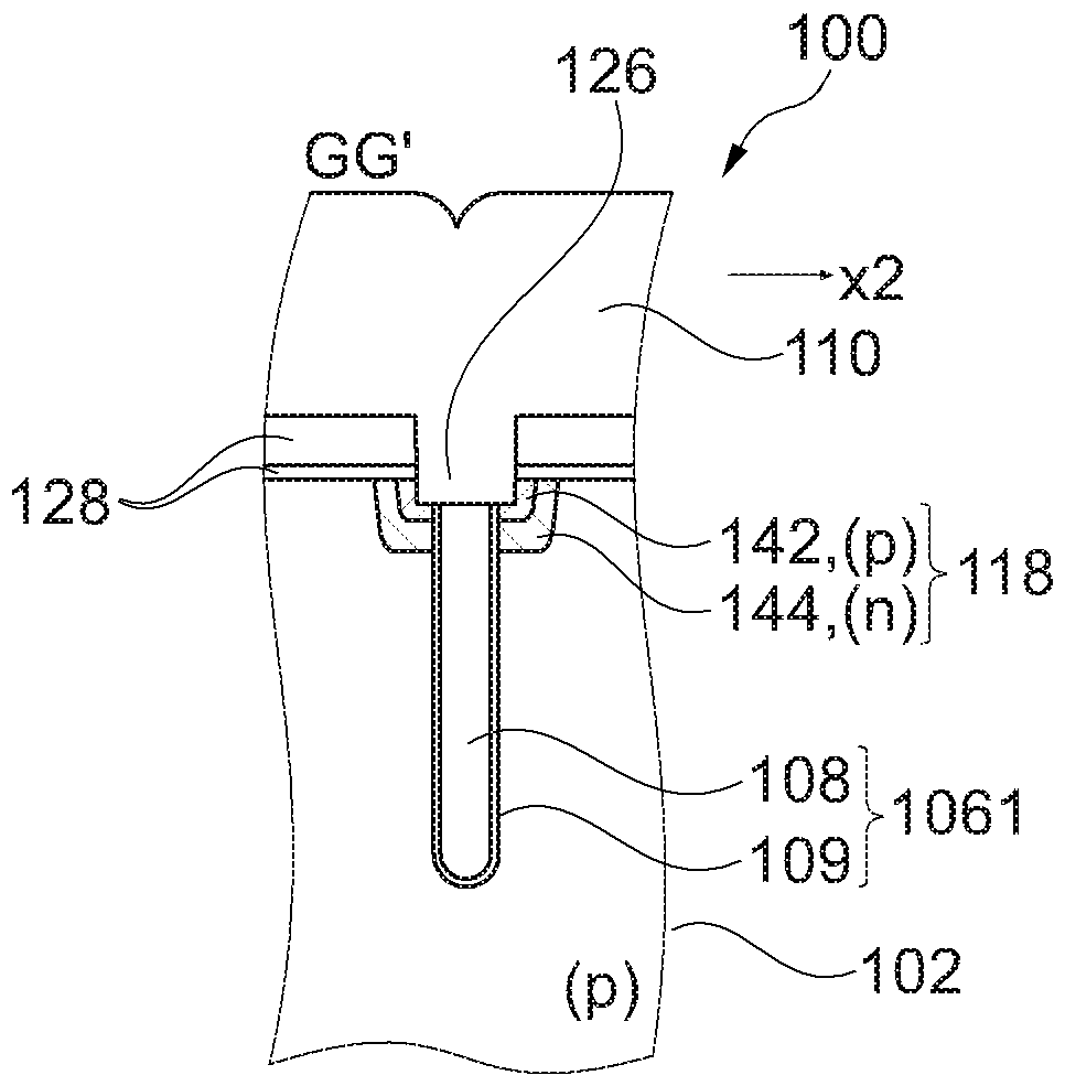
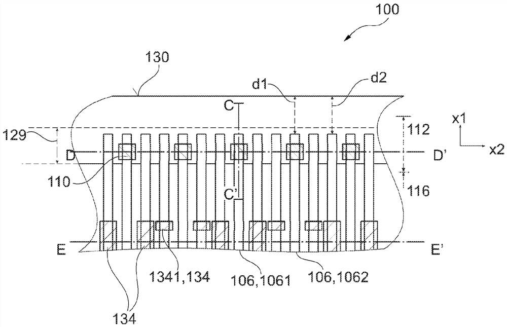
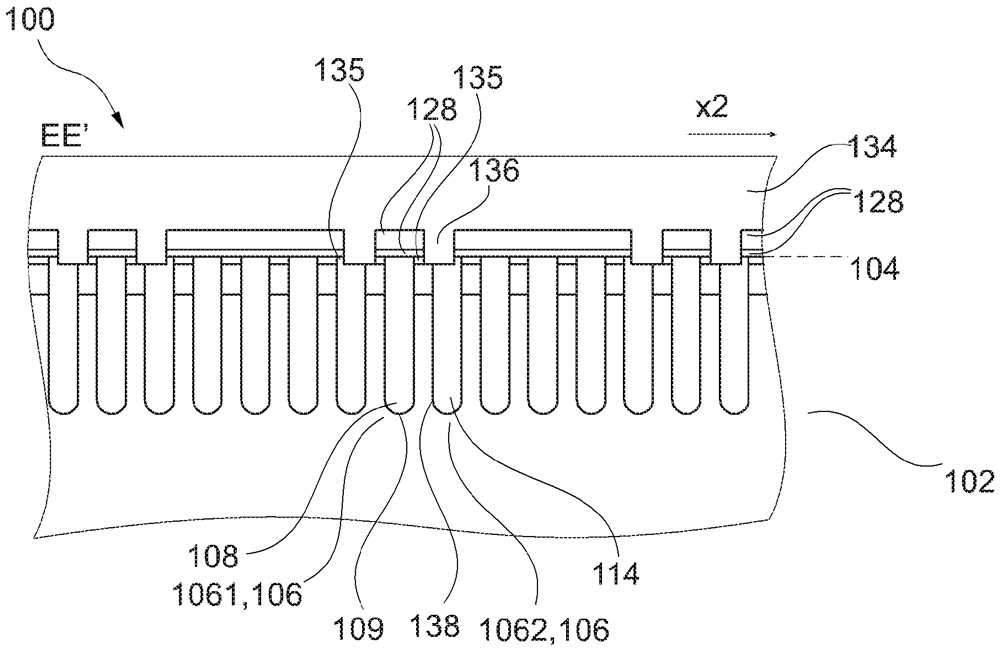
[0015] In the following detailed description, reference is made to the accompanying drawings, which form a part hereof, and in which are shown by way of illustration specific embodiments in which semiconductor devices may be practiced. It is to be understood that other embodiments may be utilized and structural or logical changes may be made without departing from the scope of the present disclosure. For example, features illustrated or described with respect to one embodiment can be used on or in conjunction with other embodiments to yield still a further embodiment. It is intended that the present disclosure includes such modifications and variations. The examples have been described using specific language, which should not be construed as limiting the scope of the appending claims. The drawings are not to scale and are for illustrative purposes only. If not stated otherwise, corresponding elements are designated by the same reference numerals in the different figures.

...


PUM


Abstract

A semiconductor device including a trench electrode structure is disclosed. The semiconductor device (100) is proposed. A semiconductor device (100) includes a semiconductor body (102), the semiconductor body (102) including a first major surface (104). The plurality of trench electrode structures (1061, 1062, 106) extend in parallel along a first lateral direction (x1). A first trench electrode structure (1061) of the plurality of trench electrode structures (1061, 1062, 106) includes a gate electrode (108). The gate contact (110) is electrically connected to the gate electrode (108) in the gate contact region (112). The gate contact region (112) is arranged in the first section along a first lateral direction (x1). An isolation structure (118) is arranged between the gate contact (110) and the semiconductor body (102) in the gate contact region (112). A bottom side (120) of the isolation structure (118) is arranged along the vertical direction (y) between a bottom side (122) of a first trench electrode structure (1061) of the plurality of trench electrode structures (1061, 1062, 106) and the first main surface (104). The gate contact (110) extends in a vertical direction (y) to the first main surface (104) or below the first main surface (104).

Description

technical field [0001] The present disclosure relates to semiconductor devices, and more particularly to semiconductor devices including trench electrode structures. Background technique [0002] Semiconductor devices such as insulated gate bipolar transistors (IGBTs) or insulated gate field effect transistors (IGFETs) such as metal oxide semiconductor field effect transistors (MOSFETs) may include trench electrode structures such as trench gate electrode structures and trench Slot source electrode structure. The electrodes in the trench electrode structure may be electrically connected in an electrode contact area, such as a gate electrode contact area or a source electrode contact area. Scaling semiconductor devices to smaller dimensions may come with more challenging contacts to electrodes. For example, when scaling semiconductor devices to smaller dimensions, manufacturing complexity and cost may increase. [0003] There is a need for improved access to electrodes in ...

Claims


Application Information

Patent Timeline
Patent Type & Authority Applications(China)
IPC IPC(8): H01L29/417H01L29/423H01L29/06H01L29/739H01L29/78H01L21/28H01L21/336H01L21/331
CPCH01L29/7827H01L29/7396H01L29/7397H01L29/66666H01L29/66348H01L29/6634H01L29/401H01L29/4236H01L29/41708H01L29/41741H01L29/0646H01L23/4824H01L29/407H01L29/0696H01L29/4238H01L29/0649H01L29/417H01L29/7813H01L29/66734H01L21/76224H01L21/76202H01L29/0653H01L23/482H01L21/761
Inventor A·卡穆斯
Owner INFINEON TECH AUSTRIA AG
Learn More