
High electron mobility transistor

A high electron mobility, transistor technology, applied in circuits, electrical components, semiconductor devices, etc., can solve problems such as the decrease of electron density in two-dimensional electron gas

Pending Publication Date: 2021-03-02
UNITED MICROELECTRONICS CORP
View PDF0 Cites 3 Cited by
  • Summary
  • Abstract
  • Description
  • Claims
  • Application Information

AI Technical Summary

Problems solved by technology

However, when two different III-V semiconductors are joined, the piezoelectric polarization direction of the one with the larger lattice size will cause the electron density of the two-dimensional electron gas to decrease

Method used


Image

  • High electron mobility transistor
  • High electron mobility transistor
  • High electron mobility transistor

Examples


Embodiment Construction

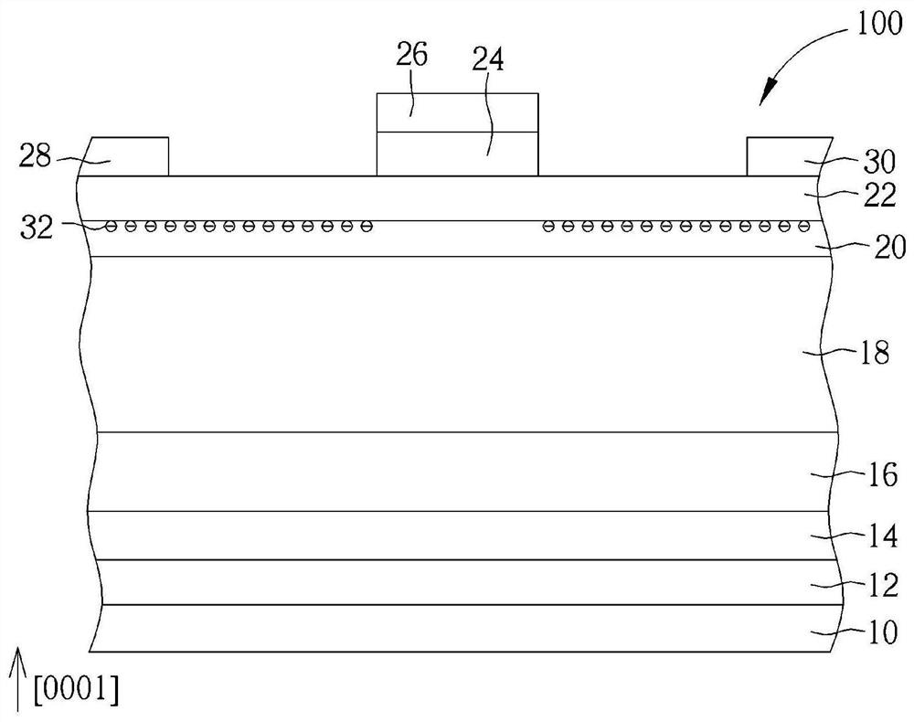
[0032] figure 1 It is a high electron mobility transistor according to the first preferred embodiment of the present invention.

[0033] Such as figure 1 As shown, a high electron mobility transistor 100 includes a substrate 10, such as a silicon substrate. A nucleation layer 12 is arranged on the silicon substrate 10, a transition layer 14 is arranged on the nucleation layer 12, a superlattice layer 16 is arranged on the transition layer 14, a zinc oxide (ZnO) layer 18 is arranged on the superlattice (superlattice) layer 16, a gallium nitride (GaN) layer 20 is arranged on the zinc oxide layer 18 and the gallium nitride layer 20 contacts the zinc oxide layer 18, an aluminum gallium nitride (Al x Ga 1-x The N) layer 22 is disposed on the GaN layer 20 and the AlGaN layer 22 contacts the GaN layer 20, and a P-type GaN layer 24 is disposed on the AlGaN layer. A gate electrode 26 is disposed on the P-type GaN layer 24 , a source electrode 28 and a drain electrode 30 are dispose...


PUM


Abstract

The invention discloses a high electron mobility transistor. The transistor comprises an aluminum gallium nitride layer, a gallium nitride layer arranged below the aluminum gallium nitride layer, a zinc oxide layer arranged below the gallium nitride layer, a source electrode and a drain electrode which are arranged on the AlGaN layer, and a gate electrode arranged on the aluminum gallium nitride layer and located on the source electrode and the drain electrode.

Description

technical field [0001] The invention relates to a high electron mobility transistor, in particular to a high electron mobility transistor in which a zinc oxide layer or a magnesium oxide layer is arranged under a channel layer. Background technique [0002] Group III-V semiconductor compounds can be applied to form many kinds of integrated circuit devices due to their semiconducting properties, such as high power field effect transistors, high frequency transistors or high electron mobility transistors. In a high electron mobility transistor, two semiconductor materials with different band-gap are joined to form a heterojunction at the junction to provide a channel for carriers. [0003] The high electron mobility transistor generates a two-dimensional electron gas (two-dimensional electron gas, 2DEG) from the material properties of the material itself, and its electron velocity and density are both high, so it can be used to increase the switching speed. However, when two ...

Claims


Application Information

Patent Timeline
IPC IPC(8): H01L29/778H01L29/267
CPCH01L29/7786H01L29/267H01L29/2003H01L29/1066H01L29/207H01L29/42316H01L29/7787H01L29/205H01L29/04H01L29/155
Inventor 许祐铭王裕齐陈彦兴杨宗穆王俞仁
Owner UNITED MICROELECTRONICS CORP
Learn More