Radio frequency filter and manufacturing method thereof
A technology of radio frequency filter and manufacturing method, which is applied in the direction of electrical components, impedance networks, etc., can solve the problems of frequency temperature coefficient increase and BAW radio frequency filter not working normally, and achieve the effect of low frequency temperature coefficient and stable performance
- Summary
- Abstract
- Description
- Claims
- Application Information
AI Technical Summary
Problems solved by technology
Method used
Image
Examples
Embodiment 1
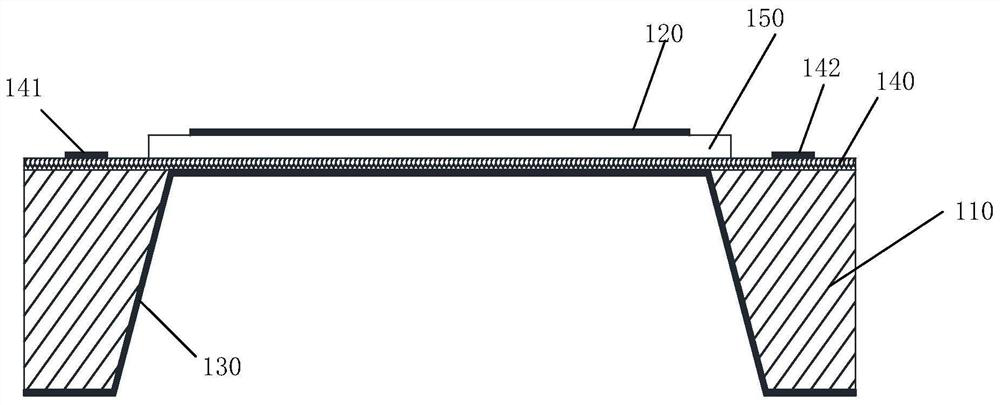
[0027] This embodiment provides a radio frequency filter, figure 1 It is a schematic cross-sectional structure diagram of a radio frequency filter provided by the present invention, refer to figure 1 The radio frequency filter provided in this embodiment includes: a substrate 110, an upper electrode layer 120, a lower electrode layer 130, a heating layer 140, and a gallium nitride layer 150; the substrate 110 includes a via region; the lower electrode layer 130 is arranged on the substrate One side of the bottom 110; the heating layer 140 is arranged on the side of the substrate 110 away from the lower electrode layer 130, and the lower electrode layer 130 and the heating layer 140 are in contact with the through hole area; the gallium nitride layer 150 is arranged on the heating layer 140 away from the substrate One side of the bottom 110 ; the upper electrode layer 120 is disposed on the side of the gallium nitride layer 150 away from the substrate 110 .
[0028] Specifical...
Embodiment 2
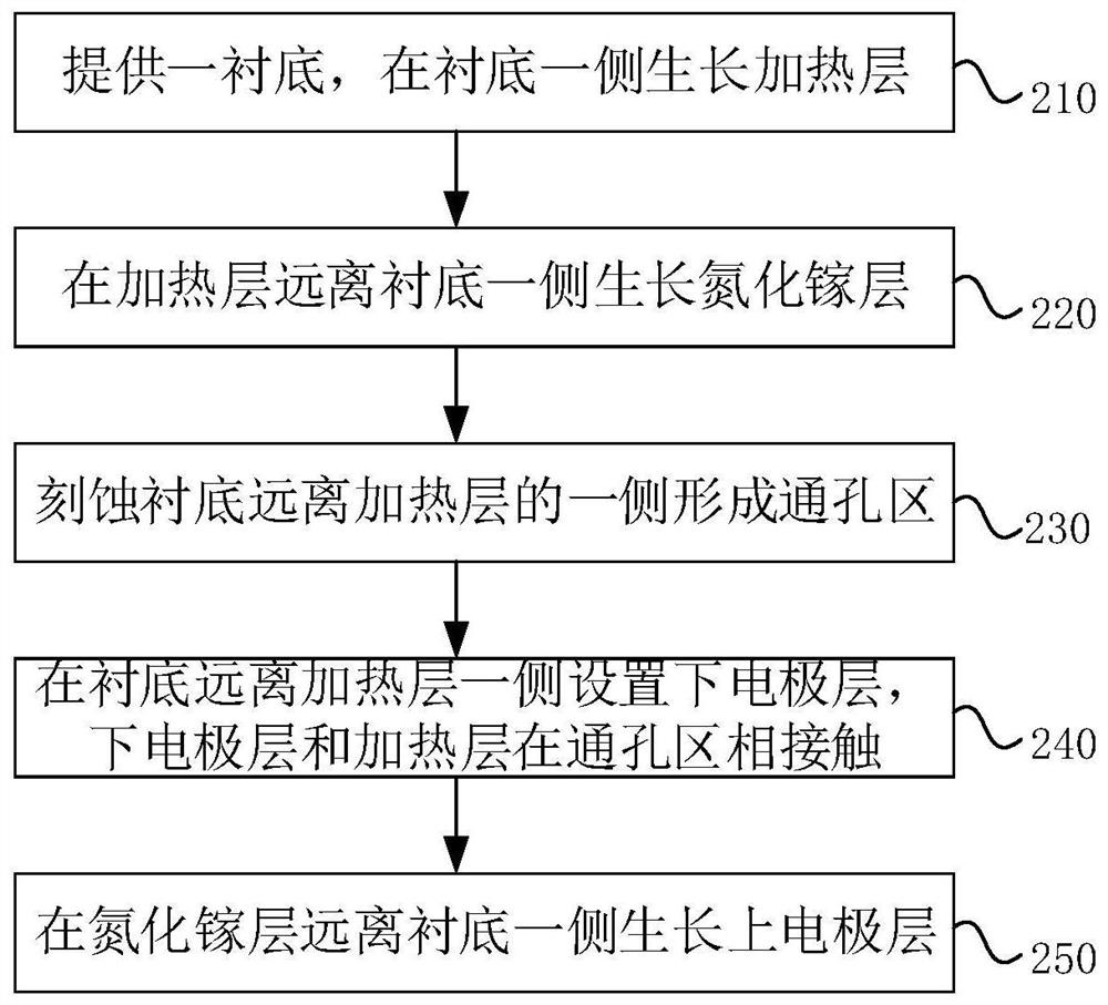
[0042] figure 2 It is a flow chart of a method for manufacturing a radio frequency filter provided by the present invention. This embodiment also provides a method for manufacturing a radio frequency filter. Refer to figure 2 , the method includes:
[0043] Step 210, providing a substrate, and growing a heating layer on one side of the substrate;
[0044] Step 220, growing a gallium nitride layer on the side of the heating layer away from the substrate;
[0045] Step 230, etching the side of the substrate away from the heating layer to form a via area;
[0046] Step 240, setting the lower electrode layer on the side of the substrate away from the heating layer, and the lower electrode layer and the heating layer are in contact with each other in the through hole area;
[0047] Step 250 , growing an upper electrode layer on the side of the gallium nitride layer away from the substrate.
[0048] The method for making a radio frequency filter provided in this embodiment, th...
PUM
| Property | Measurement | Unit |
|---|---|---|
| Thickness | aaaaa | aaaaa |
Abstract
Description
Claims
Application Information
 - R&D Engineer
- R&D Manager
- IP Professional
- Industry Leading Data Capabilities
- Powerful AI technology
- Patent DNA Extraction
Browse by: Latest US Patents, China's latest patents, Technical Efficacy Thesaurus, Application Domain, Technology Topic, Popular Technical Reports.
© 2024 PatSnap. All rights reserved.Legal|Privacy policy|Modern Slavery Act Transparency Statement|Sitemap|About US| Contact US: help@patsnap.com


