
Diode packaging process and packaging diodes

A technology for encapsulating diodes and encapsulation processes, applied in semiconductor devices, electrical components, battery temperature control, etc., can solve problems such as the inability to protect the internal structure of light-emitting diodes, achieve small shape changes, increase luminous flux output, and improve luminous efficiency Effect

Active Publication Date: 2022-03-22
ZHONGSHAN JUMINGXING ELECTRONICS
View PDF9 Cites 0 Cited by
  • Summary
  • Abstract
  • Description
  • Claims
  • Application Information

AI Technical Summary

Problems solved by technology

[0003] The embodiment of the present application provides a diode packaging process and a packaged diode, which can solve the problem that the internal structure of the light-emitting diode cannot be well protected by using the prior art packaging process to manufacture light-emitting diodes

Method used


Image

  • Diode packaging process and packaging diodes
  • Diode packaging process and packaging diodes
  • Diode packaging process and packaging diodes

Examples


Embodiment Construction

[0048] In the following description, specific details such as specific system structures and technologies are presented for the purpose of illustration rather than limitation, so as to thoroughly understand the embodiments of the present application. It will be apparent, however, to one skilled in the art that the present application may be practiced in other embodiments without these specific details. In other instances, detailed descriptions of well-known systems, devices, circuits, and methods are omitted so as not to obscure the description of the present application with unnecessary detail.

[0049] It should be understood that when used in this specification and the appended claims, the term "comprising" indicates the presence of described features, integers, steps, operations, elements and / or components, but does not exclude one or more other Presence or addition of features, wholes, steps, operations, elements, components and / or collections thereof.

[0050] It should...


PUM


Abstract

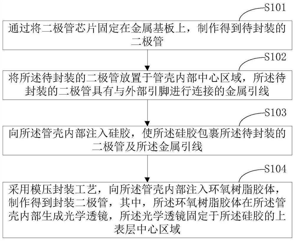
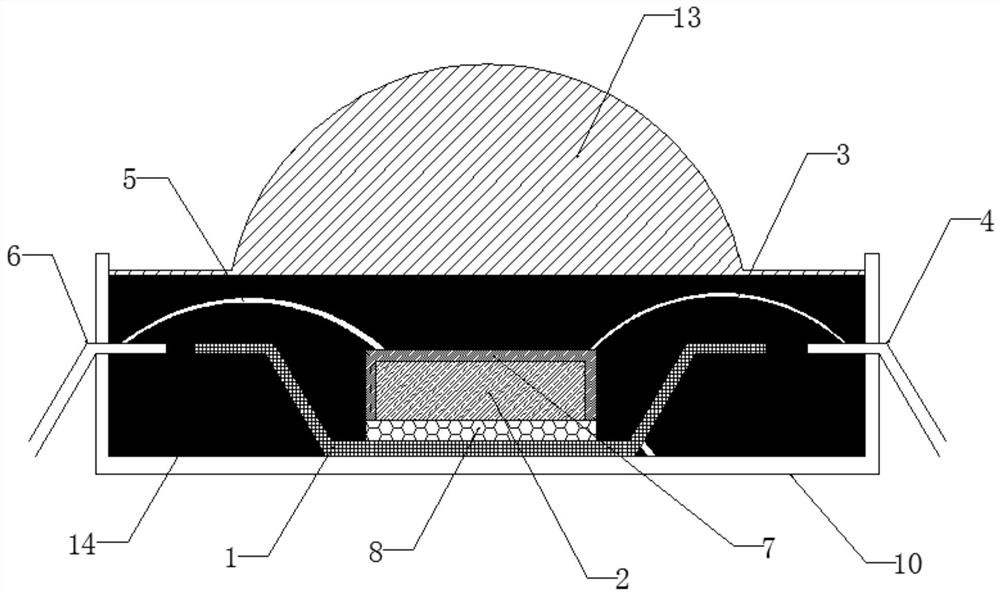
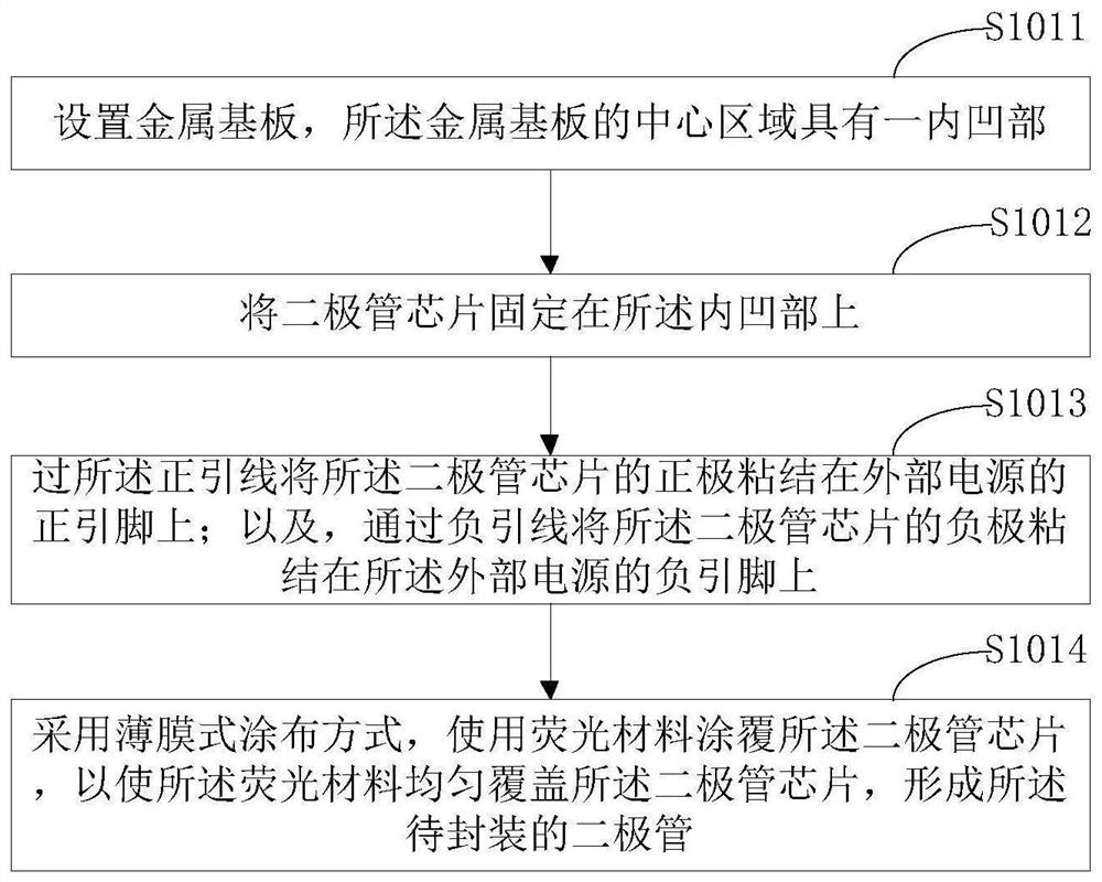
This application is applicable to the technical field of diode packaging, and provides a diode packaging process and packaged diodes, wherein, the process includes: making a diode to be packaged by fixing the diode chip on a metal substrate; placing the diode to be packaged In the central area inside the tube shell, the diode to be packaged has metal leads connected to the external pins; inject silicone into the inside of the tube shell, so that the silicone gel wraps the diode to be packaged and the metal lead; The epoxy resin colloid is manufactured to package the diode, wherein the epoxy resin colloid forms an optical lens inside the tube shell, and the optical lens is fixed on the central area of ​​the upper surface of the silica gel. By wrapping the diode to be packaged and the metal lead with silica gel, the structure of the metal lead in the package diode can be protected from being broken even if the package diode is in a high-temperature working state.

Description

technical field [0001] The application belongs to the technical field of diode packaging, and in particular relates to a diode packaging process and a packaged diode. Background technique [0002] Traditional high-power light-emitting diode packaging technology uses epoxy resin as the packaging colloid to package the light-emitting diode chip in the mold. The light-emitting diodes will generate a lot of heat when they work, so that the thermal expansion and contraction of the metal wires connected to the external pins in the light-emitting diode chips are inconsistent with the thermal expansion and contraction of the epoxy resin, which will easily cause the metal wires to be pulled off and cause damage to the light-emitting diodes. By adding a curing material into the epoxy resin to cure the epoxy resin, the probability of the metal being broken can be reduced. However, adding curing materials into the epoxy resin will easily change the light conductivity of the epoxy resin...

Claims


Application Information

Patent Timeline
Patent Type & Authority Patents(China)
IPC IPC(8): H01L33/48H01L33/52H01L33/56H01L33/62H01L33/58H01M10/64
CPCH01L33/48H01L33/52H01L33/56H01L33/62H01L33/58H01L33/641Y02E60/10
Inventor 李志源郭小明
Owner ZHONGSHAN JUMINGXING ELECTRONICS
Learn More