Double-gap electromagnetic shielding system, design method thereof and microwave circuit

A technology of electromagnetic shielding and design method, applied in the fields of magnetic field/electric field shielding, shielding materials, electrical components, etc., can solve problems such as uncorrectable, single-gap electromagnetic shielding structure difficult to apply microwave, millimeter wave circuit upgrade and transformation, large structure thickness, etc.

Active Publication Date: 2021-03-09
XIDIAN UNIV
View PDF17 Cites 1 Cited by
  • Summary
  • Abstract
  • Description
  • Claims
  • Application Information

AI Technical Summary

Problems solved by technology

[0006] (1) The periodic metal pillars of the existing single-gap electromagnetic shielding structure need to be integrally processed on one of the two metal surfaces that need to be in contact. The electromagnetic shielding structure needs to be designed in advance and cannot be corrected later
[0007] (2) The single-gap electromagnetic shielding structure is dif

Method used


Image

  • Double-gap electromagnetic shielding system, design method thereof and microwave circuit
  • Double-gap electromagnetic shielding system, design method thereof and microwave circuit
  • Double-gap electromagnetic shielding system, design method thereof and microwave circuit

Examples


Embodiment 1

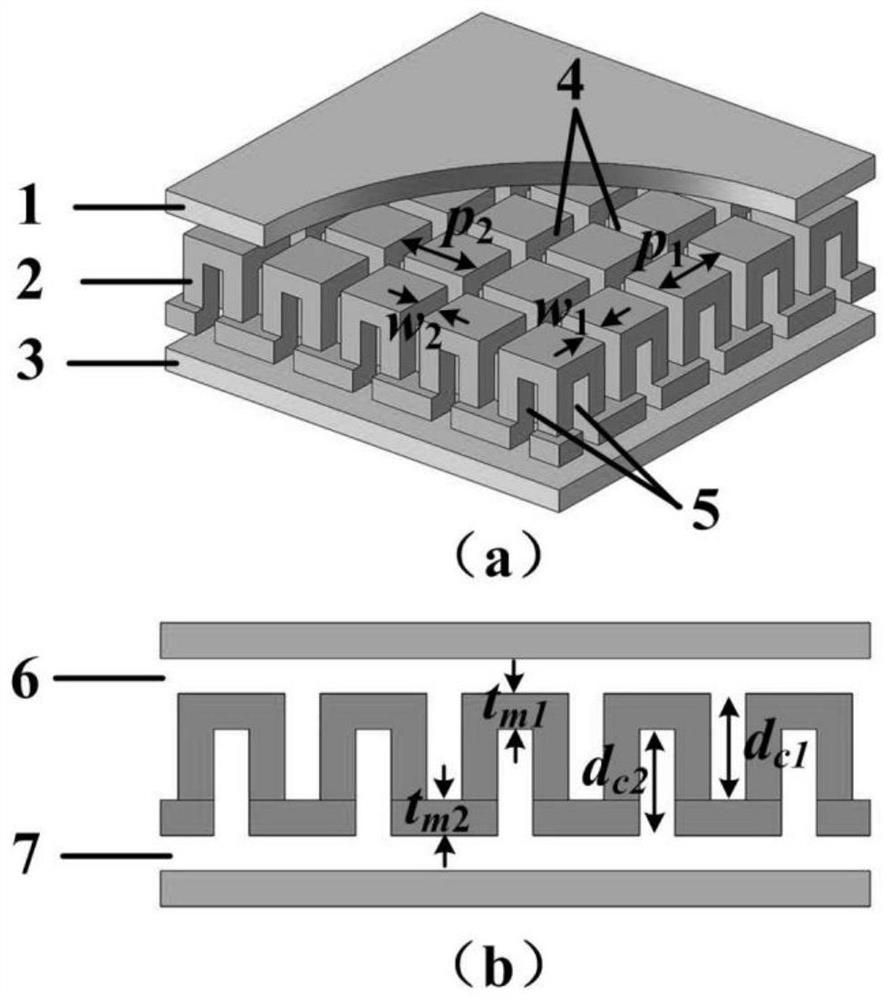
[0085] Such as figure 1 As shown, the double-gap electromagnetic shielding system provided by the embodiment of the present invention at least includes: a first metal plate, a second metal plate, a third metal plate, the first horizontal and vertical rectangular slots on the front of the second metal plate, the second metal plate Second transverse and longitudinal rectangular slots on the back, a first air gap between the first metal plate and the second metal plate, a second air gap between the third metal plate and the second metal plate.

[0086] Such as Figure 4 As shown, the simulated dispersion diagram of the electromagnetic shielding structure, the specific size is: d c1 = d c2 =6mm,p 1 =p 2 = 4.5 mm; w 1 =w 2 = 1.2 mm; h a1 = h a2 =0.1mm; that is, t m1 = t m2 = 1mm.

Embodiment 2

[0088] Such as figure 1 As shown, the double-gap electromagnetic shielding system provided by the embodiment of the present invention at least includes: a first metal plate, a second metal plate, a third metal plate, the first horizontal and vertical rectangular slots on the front of the second metal plate, the second metal plate Second transverse and longitudinal rectangular slots on the back, a first air gap between the first metal plate and the second metal plate, a second air gap between the third metal plate and the second metal plate.

[0089] Such as Figure 5 As shown, the simulated dispersion diagram of the electromagnetic shielding structure, the specific size is: d c1 = d c2 =6mm,p 1 =p 2 = 4.5 mm; w 1 =w 2 = 1.2 mm; h a1 = h a2 = 0mm; that is, t m1 = t m2 = 1mm.

Embodiment 3

[0091] Such as figure 1 As shown, the double-gap electromagnetic shielding system provided by the embodiment of the present invention at least includes: a first metal plate, a second metal plate, a third metal plate, the first horizontal and vertical rectangular slots on the front of the second metal plate, the second metal plate Second transverse and longitudinal rectangular slots on the back, a first air gap between the first metal plate and the second metal plate, a second air gap between the third metal plate and the second metal plate.

[0092] Such as Figure 6 As shown, the simulated dispersion diagram of the electromagnetic shielding structure, the specific size is: d c1 = 6mm, d c2 = 4mm, p 1 =p 2 = 4.5 mm; w 1 =w 2 = 1.2 mm; h a1 = h a2 =0.1mm; that is, t m1 = t m2 = 1mm.


PUM


Abstract

The invention belongs to the technical field of microwave electronic circuits, and discloses a double-gap electromagnetic shielding system, a design method thereof and a microwave circuit. The systemcomprises a first metal plate and a second metal plate; second transverse and longitudinal rectangular grooves are formed in the back surface of the second metal plate, a first air gap is formed between the first metal plate and the second metal plate, and a second air gap is formed between the third metal plate and the second metal plate; the second metal plate is arranged between the first metalplate and the third metal plate; and the first metal plate and the third metal plate are parallel. The depths of the rectangular grooves in the two faces of the second metal plate range from 1% wavelength to 1/2 wavelength of the center frequency of the electromagnetic shielding structure. The double-gap electromagnetic shielding structure has the advantages of being compact in structure and small in thickness, and the requirement of a microwave millimeter wave circuit for miniaturization of the double-gap electromagnetic shielding structure is met. The invention can be used for improving theelectric contact performance of the microwave millimeter wave circuit and inhibiting electromagnetic radiation.

Description

technical field [0001] The invention belongs to the technical field of microwave electronic circuits, and in particular relates to a double-gap electromagnetic shielding system, a design method thereof, and a microwave circuit. Background technique [0002] At present, the closest existing technologies: microwave, millimeter wave, and terahertz circuits have strict requirements on the electrical contact performance between the sub-circuits that constitute the circuit. In order to obtain good electrical contact performance, the traditional method is to improve the smoothness of the contact surface of the sub-circuit as much as possible, and to increase the contact pressure between the contact surfaces as much as possible. Under the condition that the above measures cannot meet the requirements of electrical performance, the contact surface should be gold-plated or silver-plated. If the electrical performance requirements are still not met, the contact surface needs to be wel...

Claims


Application Information

Patent Timeline
IPC IPC(8): H05K9/00
CPCH05K9/0075
Inventor 孙冬全陈翔邓敬亚郭立新魏兵
Owner XIDIAN UNIV
Why Eureka
Try Eureka