Clamp and clamping method for semiconductor laser bars

A laser and semiconductor technology, applied in metal material coating process, vacuum evaporation coating, coating, etc., can solve the problems of mechanical center point offset, bar falling off, thermal deformation, etc., and achieve thin fixture thickness and low cost , The effect of improving processing efficiency

Active Publication Date: 2021-03-16
GUANGXUN SCI & TECH WUHAN
View PDF13 Cites 2 Cited by
  • Summary
  • Abstract
  • Description
  • Claims
  • Application Information

AI Technical Summary

Problems solved by technology

[0010] The technical problem to be solved by the embodiments of the present invention is that during the evaporation process, the bar fixture placed in the equipment will heat up accordingly. After the heat is generated, the fixture, the bar, and the spatula will all be heated and deformed to cause the mechanical center point to shift. At this time The force balance of the clamping system is disrupted, and when the deflection exceeds a threshold, the bar falls off the clamping

Method used


Image

  • Clamp and clamping method for semiconductor laser bars
  • Clamp and clamping method for semiconductor laser bars
  • Clamp and clamping method for semiconductor laser bars

Examples


Embodiment 1

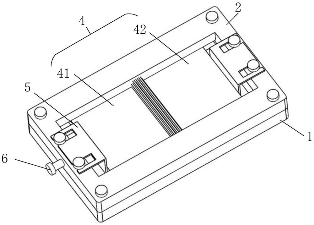
[0059] Embodiment 1 of the present invention provides a fixture for semiconductor laser bars, such as figure 1 and figure 2 As shown, it includes the lower outer frame 1 of the fixture, the upper outer frame 2 of the fixture, the step 3 for placing the bar, the bar gasket 4, the thrust shrapnel 5 and the thrust bolt 6 and, specifically:

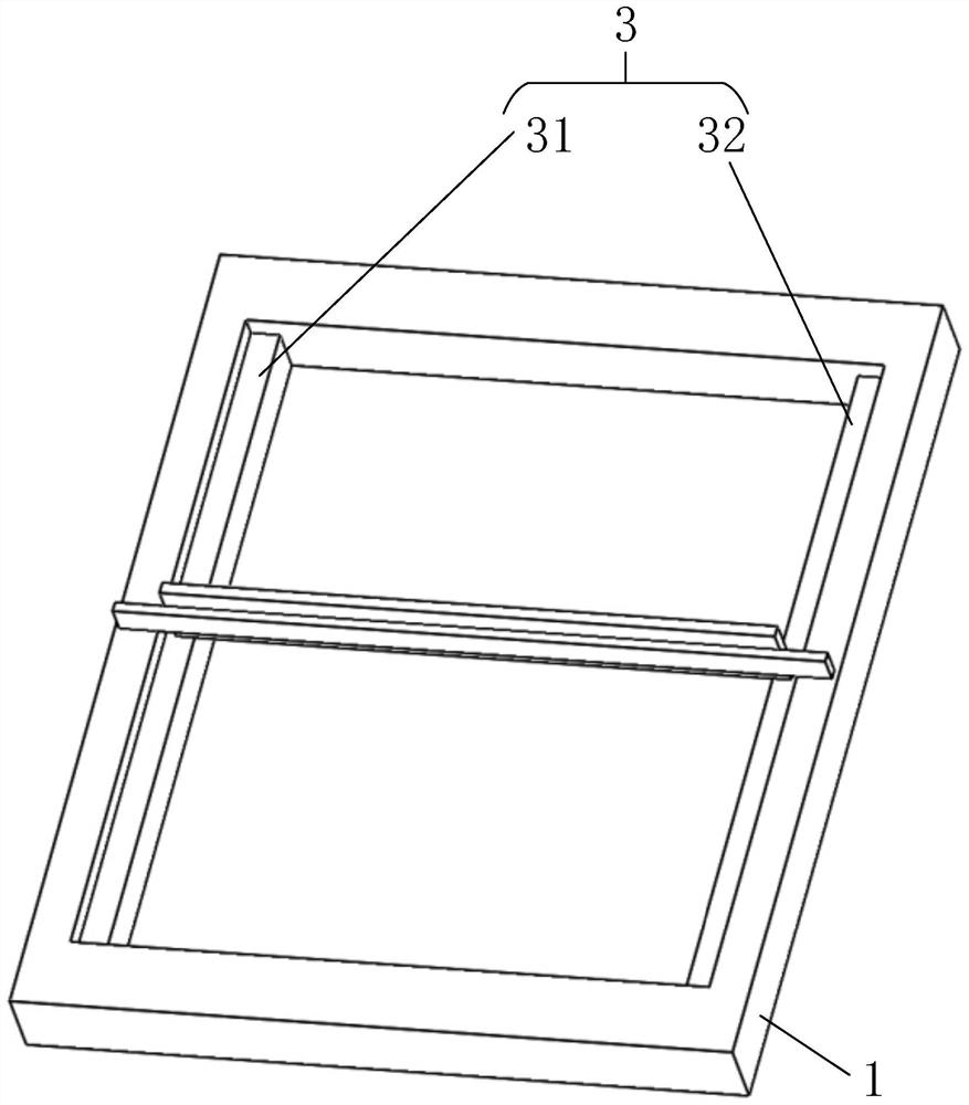
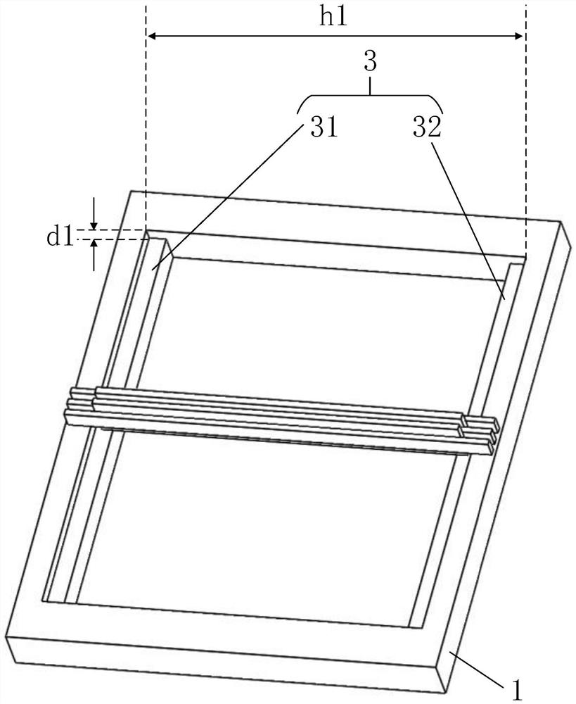
[0060] The step 3 includes a first step 31 and a second step 32, and is symmetrically arranged on opposite inner sides of the lower outer frame 1 of the fixture, and the upper surface of the step 3 is lower than the lower outer frame of the fixture. 1; wherein, the first step 31 and the second step 32 are used to hold up the two ends of the laser bar; the upper surface of the clamp lower frame (1), or the first step ( 31) and the second step (32), to hold up the positions of the two ends of the laser spar;

[0061] Described bar spacer 4 comprises first spacer 41 and second spacer 42, is arranged on described step 3 and / or fixture lower fr...

Embodiment 2

[0083] Embodiments of the present invention provide a clamping method for a semiconductor laser bar, using the clamp for a semiconductor laser bar described in Embodiment 1, such as Figure 15 As shown, clamping methods include:

[0084] In step 201, the laser bars are placed on the step 3, and the laser bars are placed on the lower frame 1 of the fixture; wherein, the placement form is that the laser bars and the laser bars are placed alternately.

[0085] In step 202, after the placement of the bar and the spatula is completed, place the bar spacer 4 on both sides of the laser bar structure to be clamped formed by the laser bar and the laser spar, and cover the fixture after the placement is completed The upper outer frame 2 is used to cover both sides of the laser spar and the bar gasket, and expose the laser bar from the middle area of ​​the upper outer frame 2 of the fixture.

[0086] In step 203 , the thrust elastic piece 5 is pushed forward by the thrust bolt 6 , so th...


PUM


Abstract

The invention relates to the technical field of semiconductor lasers, and provides a clamp and clamping method for semiconductor laser bars. The method comprises the steps that the laser bars are placed on a step, and laser accompanying bars are placed on a clamp lower outer frame, wherein the laser bars and the laser accompanying bars are alternately placed one by one; after the bars and the accompanying bars are placed, bar gaskets are placed on the two sides of a to-be-clamped laser bar structure composed of the laser bars and the laser accompanying bars, and after placing is completed, thelaser bar structure is covered with a clamp upper outer frame for shielding the two sides of the laser accompanying bar and the two sides of the bar gaskets, and the laser bars are exposed from the middle area of the clamp upper outer frame; and a thrust elastic piece is pushed forwards through a thrust bolt, so that the thrust elastic piece and the bar gaskets are attached and pressed. The clampand clamping method for the semiconductor laser bars has the advantages that loss is small, cost is low, the number of the clamped bars is large, the clamp is thick, and the bars are free of fallingrisk and the like in the later-period use process.

Description

【Technical field】 [0001] The invention relates to the technical field of semiconductor lasers, in particular to a clamp and a clamping method for semiconductor laser bars. 【Background technique】 [0002] In the era of big data and information, optical modules are widely used in current 4G, 5G communication networks, data centers and other application scenarios, and the core device in optical modules is semiconductor laser chips. Semiconductor laser chips play a key role in converting electrical signals into optical signals. [0003] According to the type of light emission, semiconductor laser chips are divided into surface emitting chips and edge emitting chips. Among them, the surface-emitting chip is mainly represented by a vertical-cavity surface-emitting laser (Vertical-Cavity Surface-Emitting Laser, referred to as: VCSEL), which is characterized in that the light-emitting surface of the laser is the upper surface of the chip. [0004] Edge-emitting chips are mainly re...

Claims


Application Information

Patent Timeline
Patent Type & Authority Applications(China)
IPC IPC(8): C23C14/50C23C14/24
CPCC23C14/50C23C14/24
Inventor 曾笔鉴万枫熊永华陈玲玲余洁陈佳俊
Owner GUANGXUN SCI & TECH WUHAN
Why Eureka
Try Eureka