Method for researching micro-discharge of double-sided dielectric loaded microwave component
A microwave component and medium loading technology, applied in electrostatic field measurement and other directions, can solve the problems of component performance degradation and functional failure
- Summary
- Abstract
- Description
- Claims
- Application Information
AI Technical Summary
Problems solved by technology
Method used
Image
Examples
Embodiment Construction
[0022] Specific embodiments of the present invention will be described in detail below in conjunction with the accompanying drawings.
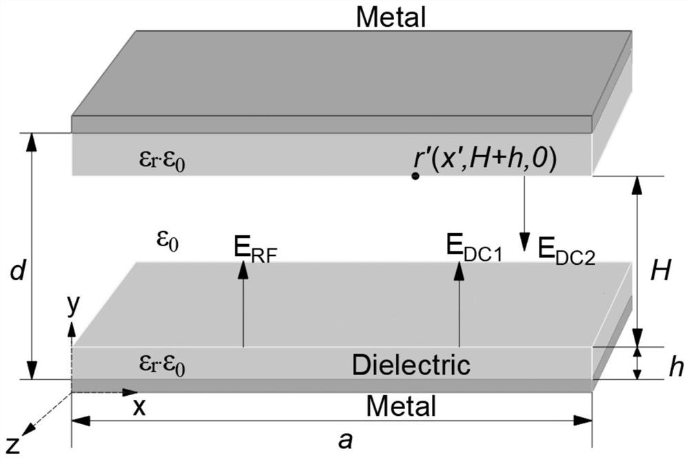
[0023] figure 1 A model diagram of a microwave component loaded with a double-sided dielectric, where the thickness of the dielectric layer is 0.05mm and the material of the dielectric layer is ferrite.
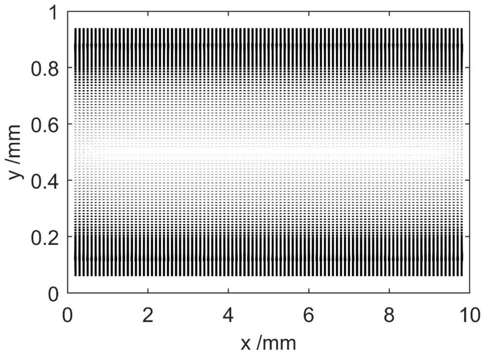
[0024] After the model is built, the charge is evenly distributed on the surface of the medium, and the distribution of the electrostatic field in the model is tested. figure 2 It is the distribution diagram of the electrostatic field in the model when the charge is uniformly distributed on the surface of the medium.
[0025] A method for micro-discharge research of double-sided dielectric loaded microwave components provided by the present invention, the main steps are as follows:
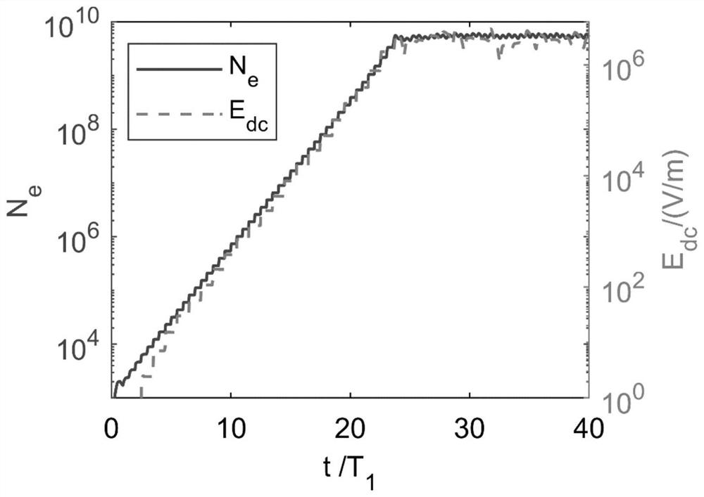
[0026] Step 1: After the test model is correct, set a cosine-changed RF electric field with vertical incidence along the surface of the medium in the model, a...
PUM
| Property | Measurement | Unit |
|---|---|---|
| Thickness | aaaaa | aaaaa |
Abstract
Description
Claims
Application Information


