
A CMOS reference voltage buffer with low output resistance

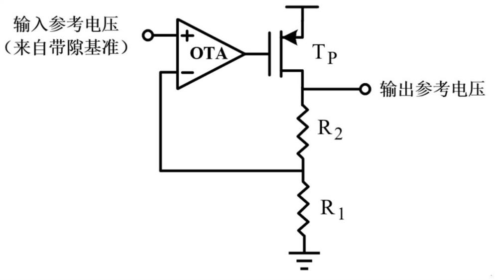
A reference voltage buffering, low output technology, applied in instruments, regulating electrical variables, control/regulating systems, etc., can solve the problems of tight voltage space, maximum limit of input reference voltage, small equivalent transconductance and output resistance, etc. Achieve the effect of small circuit overhead and low power consumption

Active Publication Date: 2022-07-01
SUZHOU UNIV
View PDF0 Cites 0 Cited by
  • Summary
  • Abstract
  • Description
  • Claims
  • Application Information

AI Technical Summary

Problems solved by technology

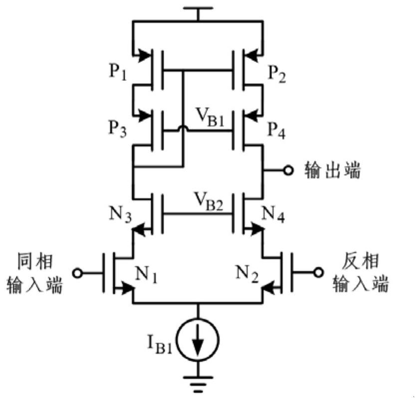
However, it has two disadvantages: (1) the maximum value of the input reference voltage is limited, and the reference voltage generated by the general reference circuit is about 1.25V; (2) the common gate stage N 3 -N 4 The bias voltage V B2 An additional bias circuit is required to meet the requirements of the operating point; (3) There is also a problem of tight voltage space in a typical analog process (180nm CMOS process), resulting in a smaller actual equivalent transconductance and output resistance, so Difficult to achieve high voltage gain
[0015] Introducing negative feedback at the common gate level to enhance the equivalent transconductance of the common gate tube is a way to increase the voltage gain, but this method requires four additional branch currents, usually used for high-speed full differential with looser power consumption constraints In the structure, such as the fully differential OTA in the pipelined high-speed ADC

Method used


Image

  • A CMOS reference voltage buffer with low output resistance
  • A CMOS reference voltage buffer with low output resistance
  • A CMOS reference voltage buffer with low output resistance

Examples


Embodiment 1

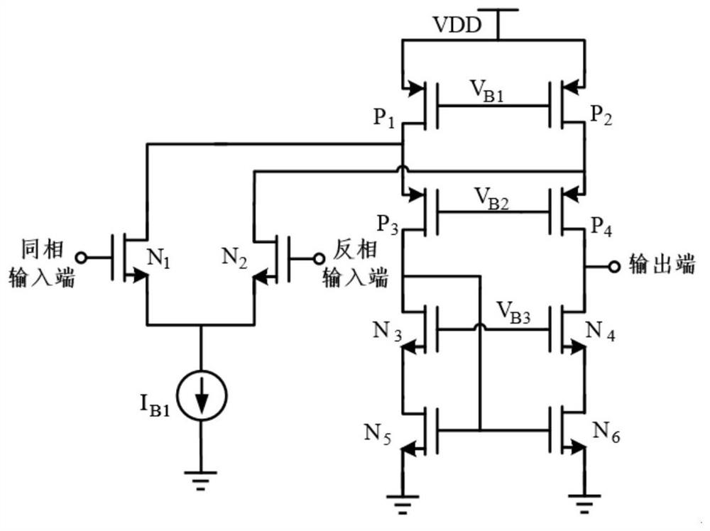
[0034] A CMOS reference voltage buffer with low output resistance, including a single-pole high-gain OTA, a power transmission PMOS transistor Tp, and a first feedback resistor R 1 and the second feedback resistor R 2 , wherein the non-inverting input terminal of the single-pole high-gain OTA inputs the reference voltage, and the inverting input terminal is connected to the first feedback resistor R 1 one end and the second feedback resistor R 2 one end, the first feedback resistor R 1 the other end of the ground, the second feedback resistor R 2 The other end of the power transmission PMOS transistor Tp is connected to the drain and outputs a reference voltage, the source of the power transmission PMOS transistor Tp is connected to the voltage source, and the gate is connected to the output terminal of the single-pole high-gain OTA. see Figure 4 As shown, the single-pole high-gain OTA includes a voltage source VDD, a first bias current source I B1 , the second bias curr...


PUM


Abstract

The invention discloses a CMOS reference voltage buffer with low output resistance. The CMOS reference voltage buffer with low output resistance includes a single-pole high-gain OTA, a power transmission PMOS transistor Tp, a first feedback resistor R1 and a second feedback Resistor R2, the single-pole high-gain OTA includes a voltage source VDD, a first PMOS transistor P1, a second PMOS transistor P2, a first NMOS transistor N1, a second NMOS transistor N2, a third NMOS transistor N3, and a fourth NMOS transistor N4 , the fifth NMOS transistor N5, the sixth NMOS transistor N6, the seventh NMOS transistor N7, the eighth NMOS transistor N8, the ninth NMOS transistor N9 and the tenth NMOS transistor N10. The reference voltage buffer provided by the present invention has a very low output impedance at a low frequency, and the extra circuit overhead is small, which is beneficial to maintain low power consumption.

Description

technical field [0001] The invention relates to the field of integrated circuit design, in particular to a CMOS reference voltage buffer with low output resistance. Background technique [0002] see figure 1 As shown, it is the basic structure of the reference voltage buffer (the filter capacitor is not shown), and its output resistance can be expressed as: [0003] [0004] where A V,OTA is the DC voltage gain of an operational transconductance amplifier (OTA), g mP Indicates the transconductance of the PMOS transistor Tp. [0005] The power consumption constraint basically determines the R 1 , R 2 and g mP The value of , so the open-loop DC voltage gain of the OTA determines the size of the output resistance. The higher the open-loop DC voltage gain of the OTA, the lower the output resistance can be achieved. In addition, in order to ensure stability, the OTA here must also be unipolar. Therefore, the cascode structure is the basic structure choice for OTA. If...

Claims


Application Information

Patent Timeline
Patent Type & Authority Patents(China)
IPC IPC(8): G05F1/56
CPCG05F1/56
Inventor 白春风马玉良殷琪浩乔东海
Owner SUZHOU UNIV
Learn More