Array substrate and manufacturing method thereof
A technology of an array substrate and a manufacturing method, applied in the field of panel display, can solve the problems of inability to effectively contact pixel electrodes 18, large step difference, and missing common electrodes 16, etc.
- Summary
- Abstract
- Description
- Claims
- Application Information
AI Technical Summary
Problems solved by technology
Method used
Image


Examples
no. 1 example
[0037] The manufacturing method of the array substrate of the present invention, such as image 3 and Figure 4 shown, including the following steps:
[0038] S1: depositing a first metal layer on the glass substrate 11, and etching the first metal layer to form a patterned gate metal layer 12;
[0039] S2: depositing the gate insulating layer 13 covering the gate metal layer 12;
[0040] S3: forming a semiconductor layer (not shown) on the gate insulating layer 13;
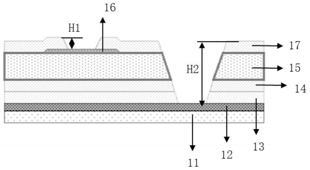
[0041] S4: depositing a second metal layer, etching the second metal layer to form a source electrode and a drain electrode respectively in contact with the semiconductor layer, and a source-drain pad layer 14 located above the semiconductor layer, the length of the source-drain pad layer 14 is d1 ;
[0042] S5: depositing the first insulating layer 15 covering the second metal layer;
[0043] S6: First deposit the organic insulating layer 16 covering the first insulating layer 15; then etch the organic insu...
no. 2 example
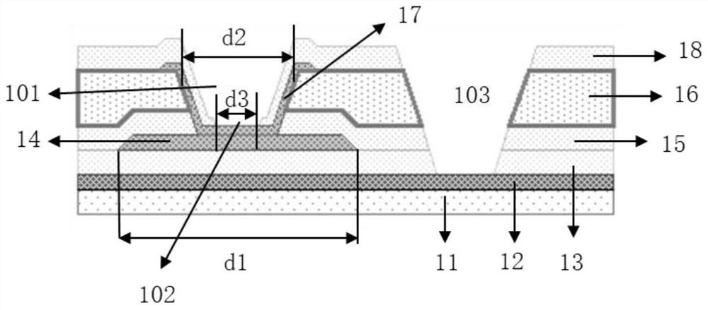
[0049] Second embodiment: as Figure 5 and Image 6 As shown, the difference from the above-mentioned first embodiment is: in step S8, the second insulating layer 18 and the common electrode 17 located in the first contact hole 101 are etched to form a second contact located on the source-drain pad layer 14 hole 102 .
[0050] That is to say, the common electrode 17 is etched when the second contact hole 102 is formed in the second embodiment. The specific manufacturing method of the second embodiment includes the following steps:
[0051] S1: depositing a first metal layer on the glass substrate 11, and etching the first metal layer to form a patterned gate metal layer 12;
[0052] S2: depositing the gate insulating layer 13 covering the gate metal layer 12;
[0053] S3: forming a semiconductor layer (not shown) on the gate insulating layer 13;
[0054] S4: depositing a second metal layer, etching the second metal layer to form a source electrode and a drain electrode respe...
PUM
 Abstract
Description
Claims
Application Information
 - R&D
- Intellectual Property
- Life Sciences
- Materials
- Tech Scout
- Unparalleled Data Quality
- Higher Quality Content
- 60% Fewer Hallucinations
Browse by: Latest US Patents, China's latest patents, Technical Efficacy Thesaurus, Application Domain, Technology Topic, Popular Technical Reports.
© 2025 PatSnap. All rights reserved.Legal|Privacy policy|Modern Slavery Act Transparency Statement|Sitemap|About US| Contact US: help@patsnap.com