Display substrate, display device and high-precision metal mask plate

A display substrate and display device technology, which is applied in metal material coating process, vacuum evaporation plating, coating, etc., can solve the problems of distortion, graininess, uneven arrangement of virtual pixel brightness centers, etc.

Pending Publication Date: 2021-03-19
BOE TECH GRP CO LTD +1
View PDF0 Cites 3 Cited by
  • Summary
  • Abstract
  • Description
  • Claims
  • Application Information

AI Technical Summary

Problems solved by technology

[0004] In view of this, the present disclosure provides a display substrate, a display device, and a high-precision metal mask, which are used to solve the uneven arrangeme

Method used


Image

  • Display substrate, display device and high-precision metal mask plate
  • Display substrate, display device and high-precision metal mask plate
  • Display substrate, display device and high-precision metal mask plate

Examples


Embodiment Construction

[0070] In order to make the purpose, technical solutions and advantages of the embodiments of the present disclosure clearer, the technical solutions of the embodiments of the present disclosure will be clearly and completely described below in conjunction with the accompanying drawings of the embodiments of the present disclosure. Apparently, the described embodiments are some of the embodiments of the present disclosure, not all of them. All other embodiments obtained by persons of ordinary skill in the art based on the described embodiments of the present disclosure belong to the protection scope of the present disclosure.

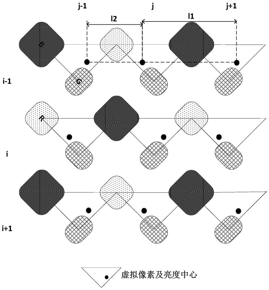
[0071] Please refer to figure 1 , figure 1 It is a schematic diagram of a pixel arrangement structure in the related art, figure 1 Both the blue sub-pixel (B) and the red sub-pixel (R) are square. Under this structure, the brightness center of the virtual pixel in the i-1th row, the jth column and the j+1th column (Fig. The distance l1 between the bl...


PUM


Abstract

The invention provides a display substrate, a display device and a high-precision metal mask plate. The display substrate comprises first sub-pixels, second sub-pixels and third sub-pixels, the firstsub-pixels and the third sub-pixels are alternately arranged in the first direction to form first sub-pixel rows, and the second sub-pixels form second sub-pixel rows; the first sub-pixel rows and thesecond sub-pixel rows are alternately arranged in the second direction; two first sub-pixels and two third sub-pixels distributed in two adjacent rows and two adjacent columns form a 2 * 2 matrix, the two first sub-pixels and the two third sub-pixels in the matrix are located in different rows and columns, the center connecting lines of the two first sub-pixels and the two third sub-pixels form avirtual quadrangle, and the second sub-pixels are located in the virtual quadrangle; and at least two of the distances from the centers of the two first sub-pixels and the centers of the two third sub-pixels in the virtual quadrangle to the center of the second sub-pixels are different. According to the invention, the arrangement of the brightness centers of the virtual pixels is more uniform.

Description

technical field [0001] The present disclosure relates to the field of display technology, in particular to a display substrate, a display device, and a high-precision metal mask. Background technique [0002] An organic light-emitting diode display (Organic light-emitting diode, OLED) display device includes a base substrate, a light-emitting layer and a package protection layer, and the light-emitting layer includes sub-pixels arranged in a matrix on the base substrate. Each sub-pixel generally vapor-deposits the organic light-emitting material on the corresponding sub-pixel position of the array substrate through a fine metal mask (FMM). With the development of technology, people have higher and higher requirements on the resolution of display devices. [0003] Currently limited to the production level of FMM and the precision of the evaporation process, it is difficult to increase the high resolution by reducing the sub-pixel size and pixel pitch. A commonly used method...

Claims


Application Information

Patent Timeline
IPC IPC(8): H01L27/32H01L51/56C23C14/24C23C14/12C23C14/04
CPCC23C14/042C23C14/24C23C14/12H10K59/352H10K59/353H10K71/164H10K71/166H10K59/122
Inventor 牛彤胡明罗昶吴建鹏王本莲嵇凤丽徐鹏徐倩张国梦黄琰
Owner BOE TECH GRP CO LTD
Why Eureka
Try Eureka