Supercharge Your Innovation With Domain-Expert AI Agents!

Microelectronic substrate warping measurement method and system based on infrared and optical images

A technology of optical image and infrared image, which is applied in the direction of optical radiation measurement, measuring device, optical device, etc., can solve the problems of inability to warp and correspond to specific positions, and achieve low cost, high synthesis accuracy, and simple equipment Effect

Pending Publication Date: 2021-03-30
HUAZHONG UNIV OF SCI & TECH
View PDF19 Cites 5 Cited by
  • Summary
  • Abstract
  • Description
  • Claims
  • Application Information

AI Technical Summary

Problems solved by technology

The rough inspection of the adjustment lever will leave scratches on the surface of the substrate. In the fine inspection, it can only judge whether the warpage is qualified, but it cannot match the warpage with the specific position.

Method used


Image

  • Microelectronic substrate warping measurement method and system based on infrared and optical images
  • Microelectronic substrate warping measurement method and system based on infrared and optical images
  • Microelectronic substrate warping measurement method and system based on infrared and optical images

Examples


Embodiment Construction

[0037] In order to make the object, technical solution and advantages of the present invention clearer, the present invention will be further described in detail below in conjunction with the accompanying drawings and embodiments. It should be understood that the specific embodiments described here are only used to explain the present invention, not to limit the present invention. In addition, the technical features involved in the various embodiments of the present invention described below can be combined with each other as long as they do not constitute a conflict with each other.

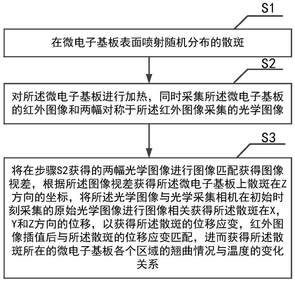
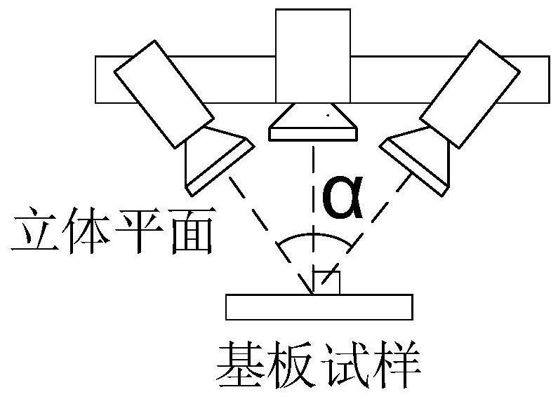
[0038] The present invention is based on the microelectronic substrate warpage measurement method of infrared and optical images, such as figure 1 As shown, the method includes steps S1-S3.

[0039] S1, sputtering randomly distributed speckles on the surface of a microelectronic substrate.

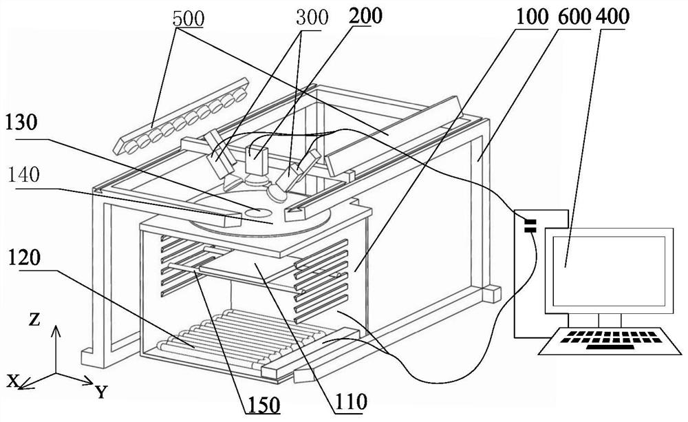
[0040] In the embodiment of the present disclosure, firstly, a matte black paint is evenly sprayed on t...


PUM


Abstract

The invention belongs to the related technical field of microelectronic substrate warping detection, and discloses a microelectronic substrate warping measurement method and system based on infrared and optical images. The method comprises the following steps: spraying randomly distributed speckles on the surface of a microelectronic substrate; heating the microelectronic substrate, and meanwhilecollecting an infrared image and an optical image of the microelectronic substrate; and carrying out image correlation on the optical image and the original optical image to obtain a displacement strain field, interpolating the infrared image, and then the infrared image having the same resolution as the optical image, thereby obtaining a change relationship between the warping condition of the microelectronic substrate where the speckle is located and the temperature. The deformation condition and the corresponding temperature condition of the microelectronic substrate are obtained by coupling the optical image and the infrared image, the relationship between the deformation amount and the temperature of the microelectronic substrate can be quantitatively obtained, the operation is simple, and the measurement is accurate.

Description

technical field [0001] The invention belongs to the related technical field of microelectronic substrate warpage detection, and more specifically relates to a microelectronic substrate warpage measurement method and system based on infrared and optical images. Background technique [0002] The temperature change during the microelectronic chip packaging process will cause the microelectronic substrate to warp and deform. In addition, the packaged chip will also experience heat warping and deformation under working conditions, and even expansion and delamination. The preparation of the microelectronic substrate and the substrate The reliability of the mounted electronic devices has a major impact. The conventional detection methods are observation method, feeler gauge measurement, etc., which are inefficient and have false detections. [0003] Chinese patent CN208606731U discloses a substrate warpage detection device, which is provided with four sensors located at four corner...

Claims


Application Information

Patent Timeline
IPC IPC(8): G01B11/16G01J5/00
CPCG01B11/16G01J5/00G01J2005/0077
Inventor 朱福龙曾宝山李金洺沈奔胡洲冯陈泽芳胡剑雄王淼操黄煜华
Owner HUAZHONG UNIV OF SCI & TECH
Features
  • R&D
  • Intellectual Property
  • Life Sciences
  • Materials
  • Tech Scout
  • Unparalleled Data Quality
  • Higher Quality Content
  • 60% Fewer Hallucinations
Learn More