AXI bus structure and chip system

A bus structure and bus technology, applied in transmission systems, bus networks, digital transmission systems, etc., can solve the problems of chip congestion and large number of interconnected bus lines, and achieve the effect of reducing the number and eliminating congestion problems.

Pending Publication Date: 2021-03-30
AXERA TECH (SHANGHAI) CO LTD
View PDF0 Cites 1 Cited by
  • Summary
  • Abstract
  • Description
  • Claims
  • Application Information

AI Technical Summary

Problems solved by technology

At the same time, multi-core also makes the number of interconnection bus lines become huge, which brings serious congestion (congestion) problems to the chip back-end implementation.

Method used


Image

  • AXI bus structure and chip system
  • AXI bus structure and chip system
  • AXI bus structure and chip system

Examples


Embodiment Construction

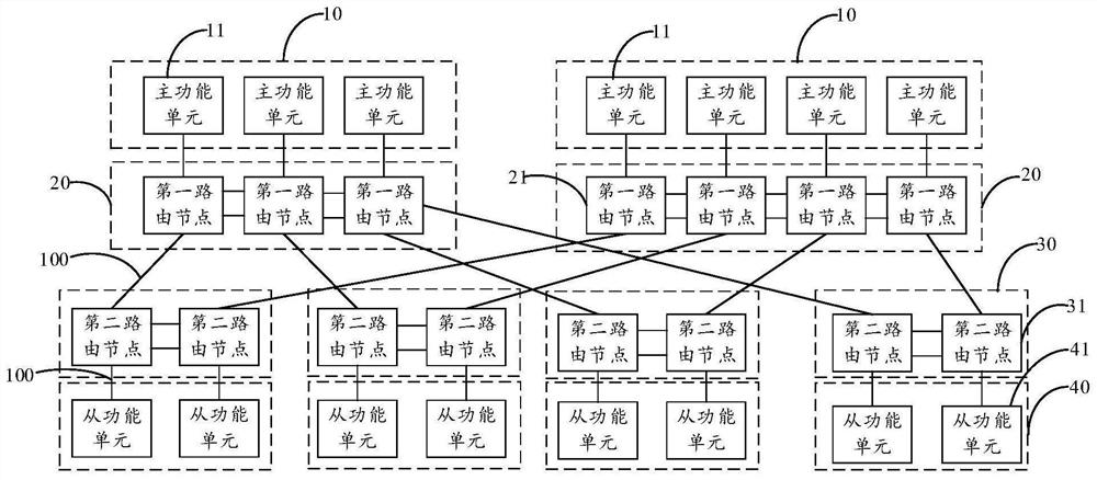
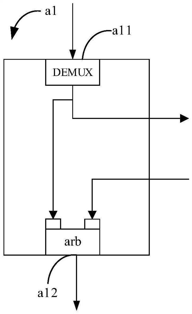
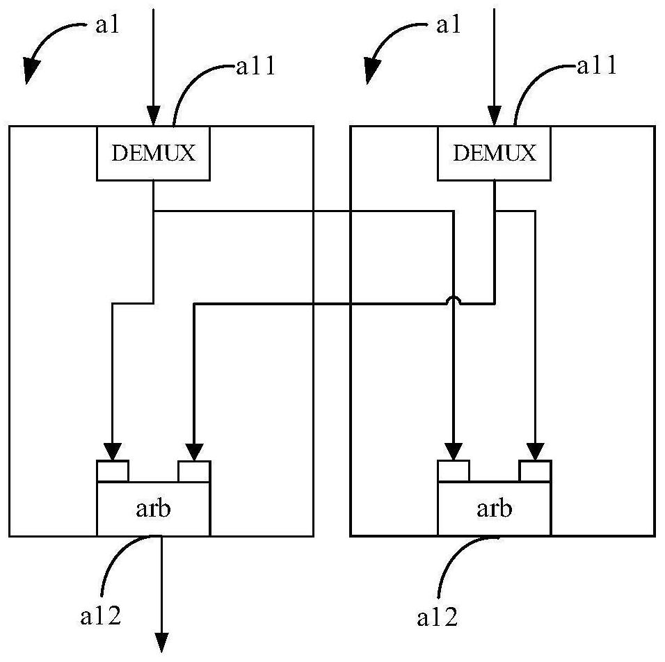
[0043] The technical solutions in the embodiments of the present application will be clearly and completely described below in conjunction with the drawings in the embodiments of the present application.

[0044]In the description of this application, it should be noted that the orientation or positional relationship indicated by the terms "inner", "outer", etc. is based on the orientation or positional relationship shown in the drawings, or the usual placement of the application product when it is used. Orientation or positional relationship is only for the convenience of describing the present application and simplifying the description, and does not indicate or imply that the referred device or element must have a specific orientation, be constructed and operated in a specific orientation, and thus should not be construed as limiting the present application. In addition, the terms "first", "second", etc. are only used for distinguishing descriptions, and should not be constr...


PUM


Abstract

The invention provides an AXI bus structure and a chip system. The AXI bus structure comprises: at least two main function unit groups, wherein each main function unit group comprises at least two main function units; at least two first routing units, wherein the at least two first routing units and the at least two main function unit groups are in one-to-one correspondence with the at least two first routing units, and each first routing unit is connected with each main function unit of the corresponding main function unit group through an AXI bus; at least two second routing units, wherein each second routing unit is connected with each first routing unit through an AXI bus; and at least two slave function unit groups, wherein each slave function unit group comprises at least two secondslave function units, the at least two slave function unit groups are in one-to-one correspondence with the at least two second routing units, and each second routing unit is connected with each slavefunction unit corresponding to the slave function unit group through an AXI bus.

Description

technical field [0001] The present application relates to the technical field of chip technology, and in particular to an AXI bus structure and a chip system. Background technique [0002] The on-chip interconnection bus (Network On Chip) refers to the connection relationship between various systems or modules in the chip, and is mainly used to realize data exchange between subsystems or functional modules in the chip. In AI processing chips, the huge data throughput requirements have brought many challenges to the design of the on-chip interconnection bus. For example, in a multi-core NPU (Neural network Processing Unit, neural network processor), the bandwidth requirements for data interaction between multiple cores and data interaction with OCM (On chip memory, on-chip storage) are huge. In order to support high bandwidth, high clock frequency and wide bus bits have become the basic characteristics of AI processor on-chip interconnection bus. At the same time, multi-cor...

Claims


Application Information

Patent Timeline
Patent Type & Authority Applications(China)
IPC IPC(8): G06F13/40G06F15/78G06F5/06H04L12/40H04L12/761H04L45/16
CPCG06F13/4031G06F13/4068G06F15/7807G06F5/06H04L12/40006H04L45/16Y02D10/00G06F13/368G06F13/42
Inventor 窦雄李毅
Owner AXERA TECH (SHANGHAI) CO LTD
Why Eureka
Try Eureka