

A kind of semiconductor device with buffer layer structure
A semiconductor and buffer layer technology, applied in the field of power semiconductor device testing, can solve the problems of device leakage current increase, avalanche breakdown, etc., and achieve the effects of reducing leakage current, reducing chip thickness, and suppressing leakage current
- Summary
- Abstract
- Description
- Claims
- Application Information
AI Technical Summary
Problems solved by technology
Method used
Image

Examples
Embodiment Construction
[0038] In order to make the purpose, technical solutions and advantages of the embodiments of the present invention more clear, the technical solutions in the embodiments of the present invention will be clearly and completely described below in conjunction with the accompanying drawings in the embodiments of the present invention. Obviously, the described embodiments It is a part of embodiments of the present invention, but not all embodiments. Based on the embodiments of the present invention, all other embodiments obtained by persons of ordinary skill in the art without making creative efforts belong to the protection scope of the present invention.
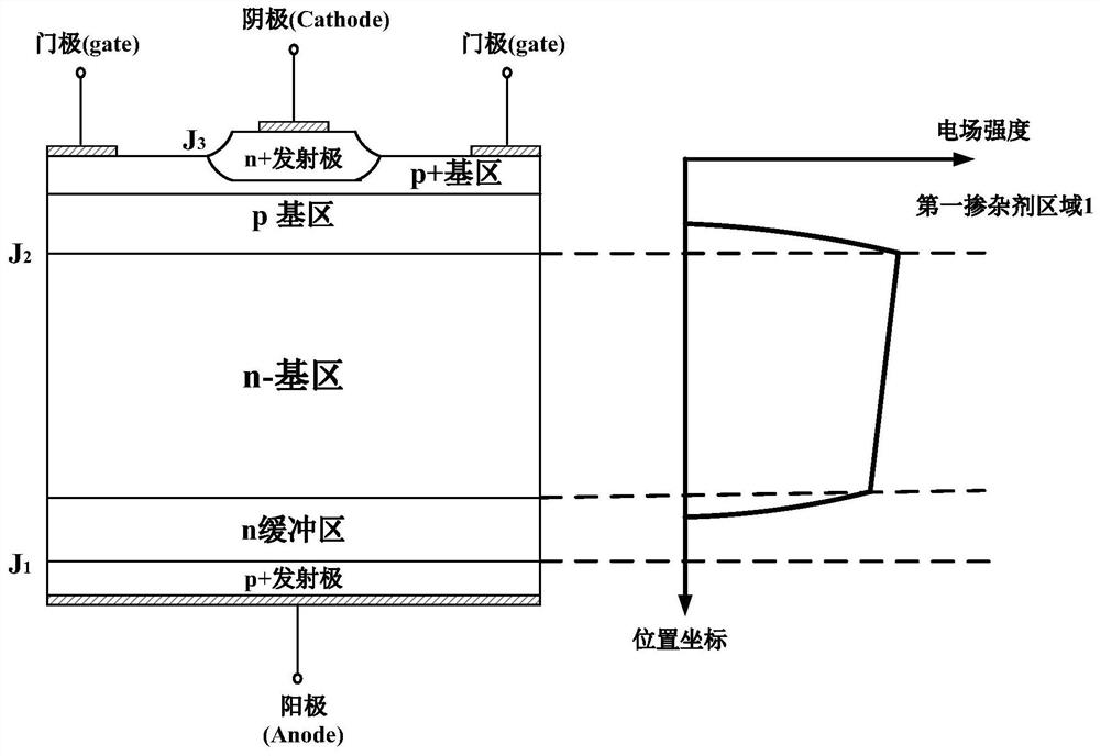
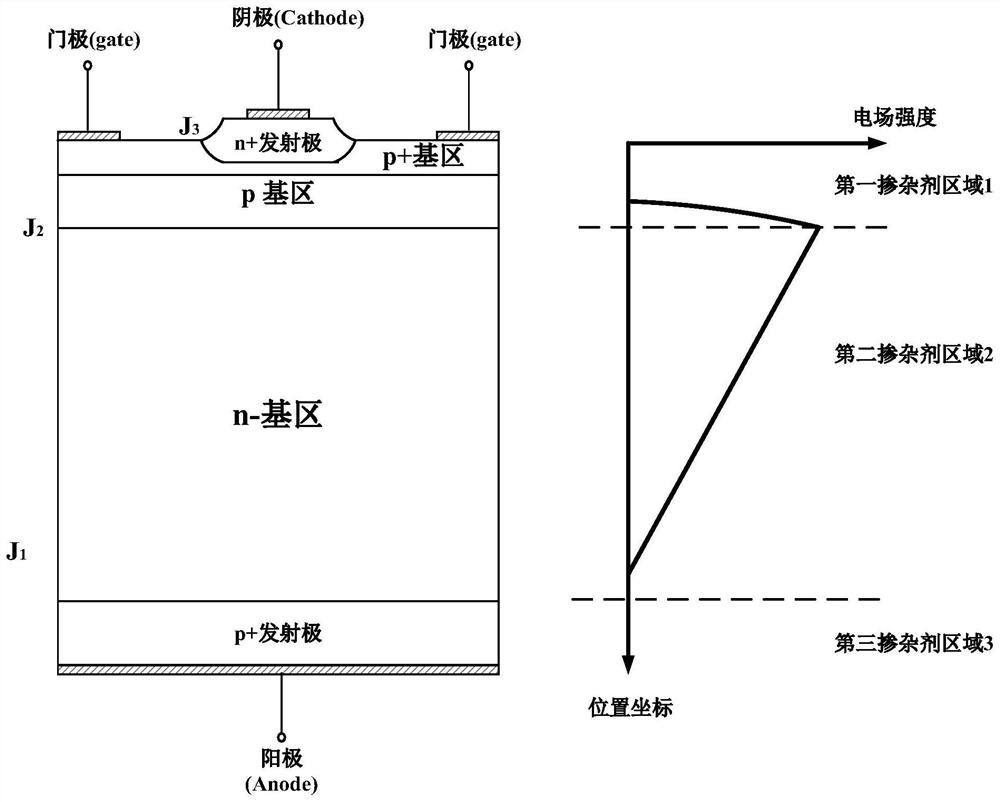
[0039] A semiconductor device with a buffer layer structure, comprising a first dopant region 1, a second dopant region 2, and a third dopant region 3 arranged in sequence, and further comprising At least one other dopant region is included between the three dopant regions 3 . Specifically, the other dopant region includes th...
PUM
| Property | Measurement | Unit |
|---|---|---|
| thickness | aaaaa | aaaaa |
Abstract
Description
Claims
Application Information