Novel Fabry-Perot tunable filter
A technology of tuning filter and Fab, applied in the field of infrared detection, can solve the problems of affecting the filtering performance, large driving voltage, large deformation, etc., achieve good filtering characteristics, meet the effect of low-voltage driving and mirror smoothness
- Summary
- Abstract
- Description
- Claims
- Application Information
AI Technical Summary
Problems solved by technology
Method used
Image

Examples
Embodiment 1
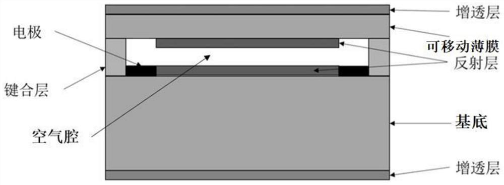
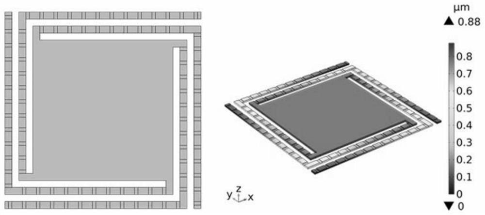
[0015] A new type of Fabry-Perot tunable filter disclosed in Embodiment 1 of the present invention adopts a double-folded cantilever beam structure, and etches the cantilever beam to form a rectangular groove. The movable thin layer refers to the Voltage generates electrostatic attraction, and moves up and down under the action of electrostatic attraction. The new Fabry-Perot tunable filter with this structure can obtain a displacement of 0.88μm at 8V, and its maximum stress is only 8.49MPa when the displacement is 0.5μm, and the mirror flatness error is only 0.9 nm. Therefore, the new Fabry-Perot filter with a rectangular slot cantilever beam can well meet the low-voltage drive, the mirror surface is flat, and it always maintains good filtering characteristics in the tunable range.
preparation example 1
[0017] The preparation process of the novel Fabry-Perot tunable filter is:
[0018] Step 1: On the upper surface of the single crystal silicon substrate, a film system of Sub / LHLHLH 6 layers alternately stacked is deposited by vacuum thermal evaporation thin film deposition process to form a reflective layer, and patterned by etching process. H and L represent a 1 / 4 central wavelength optical thickness of film layer Ge (high refractive index material layer) and film layer SiO (low refractive index material layer) respectively, central wavelength λ=4260nm, 1H=(4n H d) / λ; 1L=(4n L d) / λ.
[0019] Step 2: On the single crystal silicon substrate coated with a reflective layer, deposit a layer of gold (Au) layer as an electrode for electrostatic attraction with a magnetron sputtering deposition process, with a thickness of 300nm, and use an etching process for patterning .
[0020] Step 3: On the lower surface of the silicon substrate, a SiO film is deposited by a vacuum thermal ...
preparation example 2
[0026] The preparation process of the novel Fabry-Perot tunable filter is:
[0027] Step 1: On the lower surface of the monocrystalline silicon substrate, a SiO film is deposited by a vacuum thermal evaporation film deposition process to form an anti-reflection layer with a thickness of 1 / 4 the optical thickness of the central wavelength, and the central wavelength λ=4260nm, and patterned by an etching process change.
[0028] Step 2: On the upper surface of the single crystal silicon substrate, a film system of Sub / LHLHLH 6 layers alternately stacked is deposited by vacuum thermal evaporation thin film deposition process to form a reflective layer, and patterned by an etching process. H and L represent a 1 / 4 central wavelength optical thickness of film layer Ge (high refractive index material layer) and film layer SiO (low refractive index material layer) respectively, central wavelength λ=4260nm, 1H=(4n H d) / λ; 1L=(4n L d) / λ.
[0029] Step 3: In the electrode working area...
PUM
| Property | Measurement | Unit |
|---|---|---|
| thickness | aaaaa | aaaaa |
| depth | aaaaa | aaaaa |
| wavelength | aaaaa | aaaaa |
Abstract
Description
Claims
Application Information