Copper plating thickening process for printed circuit board

A printed circuit and board copper plating technology, applied in printed circuit, printed circuit manufacturing, electrical components, etc., can solve problems such as reliability and abnormal appearance, excessive ink side erosion, excessive burr, etc., to improve the production process ability, improve line burrs, and improve production efficiency

Active Publication Date: 2021-04-09
惠州市大亚湾科翔科技电路板有限公司
View PDF5 Cites 6 Cited by
  • Summary
  • Abstract
  • Description
  • Claims
  • Application Information

AI Technical Summary

Problems solved by technology

[0004] The purpose of the present invention is to provide a copper plating thickening process for printed circuit boards. The technical solution provided by the present invention solves the problems of the existing printed circuit boards with relatively high copper thickness in the production process of electroplating, wiring, and solder resistance. There are problems such as uneven copper plating, copper plating blocking holes, dirty etching, excessive burr, ink bubbles, excessive ink side erosion, etc., and abnormal appearance

Method used


Image

  • Copper plating thickening process for printed circuit board
  • Copper plating thickening process for printed circuit board
  • Copper plating thickening process for printed circuit board

Examples


Embodiment Construction

[0027] The following will clearly and completely describe the technical solutions in the embodiments of the present invention with reference to the drawings in the embodiments of the present invention. Apparently, the described embodiments are only some of the embodiments of the present invention, but not all of them. Based on the embodiments of the present invention, all other embodiments obtained by persons of ordinary skill in the art without creative efforts fall within the protection scope of the present invention.

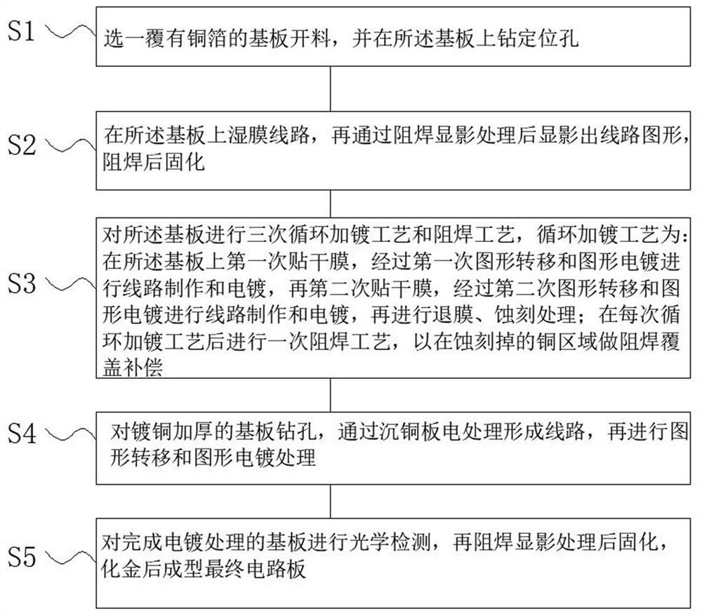
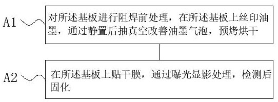
[0028] For printed circuit boards with a copper thickness of 9oz or more and a board thickness of 5.4mm, there are abnormalities such as uneven copper plating and copper-plated hole blocking during electroplating; Abnormalities such as excessive burrs; during solder mask printing, problems such as ink bubbles and excessive ink side erosion due to excessive copper thickness and excessive circuit burrs.

[0029] In order to solve the above-mentioned technical ...


PUM

PropertyMeasurementUnit
thicknessaaaaaaaaaa
thicknessaaaaaaaaaa
diameteraaaaaaaaaa

Abstract

The invention belongs to the technical field of circuit board processing and relates to a copper plating thickening process for printed circuit board. By adopting a novel cyclic plating process flow, the problem of uneven copper plating is avoided while copper plating thickening is completed, a processing method for improving uneven copper plating, incomplete etching and excessive ink lateral erosion is obtained by combining process optimization and process parameter adjustment, the production process capability is improved, the production efficiency is improved, the quality risk is reduced, and the production cost is reduced. With the method adopted, the problem that copper plating above 9 oz is difficult to thicken can be effectively solved, the abnormities of uneven copper plating, copper plating hole blockage and the like during thick copper electroplating can be avoided; and circuit burrs can be improved through multiple times of etching, and it is guaranteed that incomplete etching and excessive burrs caused by excessive copper thickness are avoided during circuit manufacturing, and therefore, the problems of ink bubbles, excessive ink lateral erosion and the like caused by overlarge copper thickness and overlarge circuit burrs during solder resist printing are effectively solved, and the product quality is greatly improved.

Description

technical field [0001] The invention relates to the technical field of circuit board processing, in particular to a copper plating and thickening process for printed circuit boards. Background technique [0002] With the rapid development of power communication technology, 4-10oz and above ultra-thick copper foil circuit boards have gradually become a type of special PCB with broad market prospects. In the process of electroplating, wiring, and solder mask production for power supply printed circuit boards, the copper thickness requirement is as high as 9oz, and the printed circuit board with a board thickness of 5.4mm has uneven copper plating and copper plating blockages during electroplating. Abnormalities such as holes; when making circuits, there are abnormalities such as unclean etching and excessive burrs due to excessive copper thickness; during solder mask printing, ink bubbles and ink side erosion are too large due to excessive copper thickness and excessive circ...

Claims


Application Information

Patent Timeline
Patent Type & Authority Applications(China)
IPC IPC(8): H05K3/18H05K3/06H05K3/00
CPCH05K3/0047H05K3/06H05K3/188
Inventor 郑晓蓉周刚王康兵
Owner 惠州市大亚湾科翔科技电路板有限公司
Why Eureka
Try Eureka