

A method of preparing microribbons or nanoribbons of two-dimensional nanomaterials
A technology of two-dimensional nanomaterials and microribbons, which is applied in photosensitive material processing, photolithographic coating equipment, semiconductor/solid-state device manufacturing, etc., can solve problems such as edge roughness, and achieve the effect of improving edge roughness
- Summary
- Abstract
- Description
- Claims
- Application Information
AI Technical Summary
Problems solved by technology
Method used
Image

Examples
example 1
[0025] Example 1: The preparation method of multilayer graphene microribbon-nanoribbon hybrid composition.
[0026] 1) Preparation of multilayer graphene by mechanical exfoliation method:
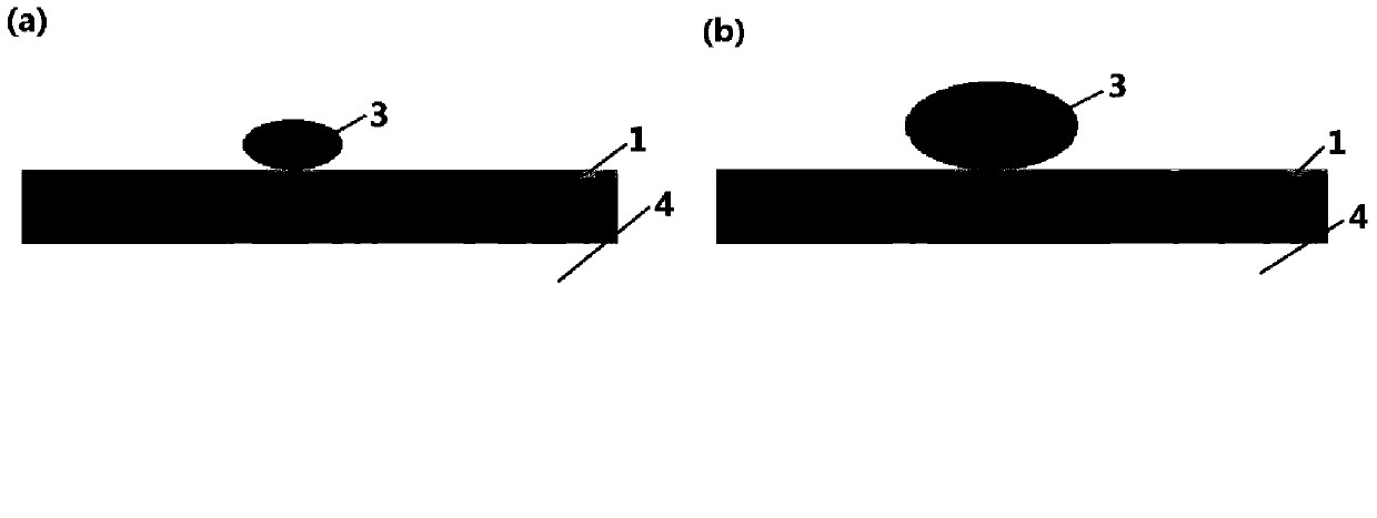
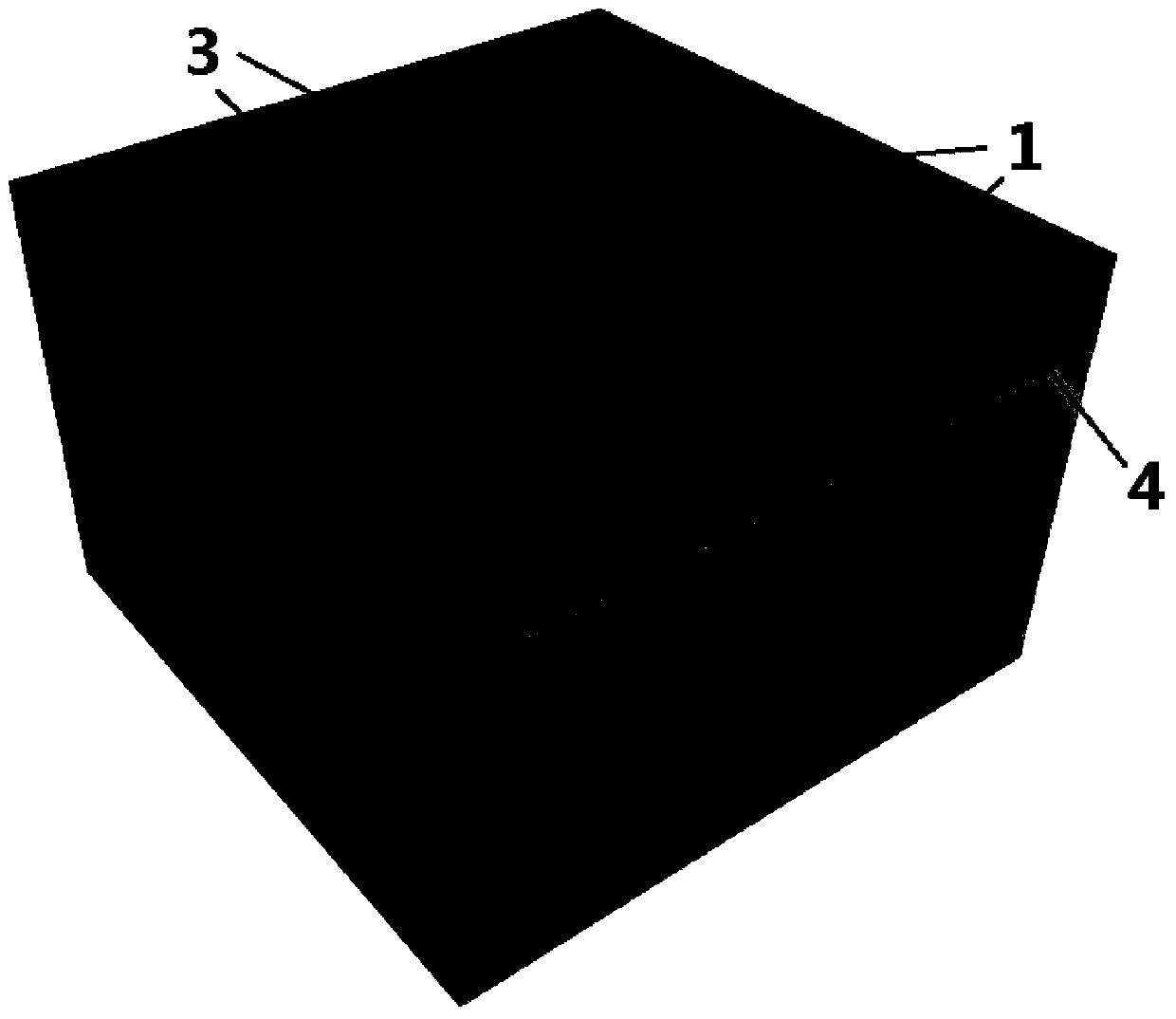
[0027] Use tape to repeatedly stick and peel off the highly oriented graphite, and finally press the tape covered with multi-layer graphene to SiO 2 / Si substrate, then there are multi-layer graphene with different thickness distributed on the whole substrate.
[0028] 2) Spin coating photoresist:
[0029] Select a water-soluble negative photoresist (AR-N 7520.18), and spin-coat it at a speed of 4000rpm for 60s to evenly cover a thinner photoresist film on the surface of the substrate. At this time, the thickness of the photoresist is about 400nm .
[0030] 3) Put the substrate into the pre-cooled developer, soak in the developer for a certain period of time, fully fix it, and blow dry:
[0031] The temperature of the substrate sheet was kept at room temperature (24°C). After cooling t...
example 2
[0036] Example 2: The preparation method of single-layer graphene nanobelt.
[0037] 1) Growth and transfer of single-layer graphene:
[0038] Using the CVD method, a single-layer continuous thin film of graphene is grown on the surface of copper foil. Spin-coat a layer of polymethyl methacrylate (PMMA) on the surface of single-layer graphene, and then put FeCl 3 After soaking in the solution until the copper foil is completely etched, transfer to SiO 2 / Si substrate. Finally, the PMMA film was dissolved with acetone, washed and dried to obtain a substrate sheet covered with single-layer graphene.
[0039]2) Spin coating photoresist:
[0040] Select a water-soluble negative photoresist (AR-N 7500.08), and spin-coat it on the surface of the sample. In order to prepare long and narrow single-layer graphene nanoribbons, it is necessary to increase the rotational speed to obtain thinner photoresist films. Therefore, the photoresist was spin-coated at a speed of 5000rpm for 6...
example 3
[0047] Example 3: Multilayer tungsten disulfide (WS 2 ) A method for preparing a microribbon-nanoribbon hybrid composition.
[0048] 1) Multilayer WS 2 Preparation of:
[0049] Use tape on WS 2 Paste on the body material and peel it off repeatedly, and finally it will be covered with multiple layers of WS 2 The tape is pressed onto the SiO 2 / Si substrate, obtained covered with multi-layer WS 2 substrate sheet.
[0050] 2) Spin coating photoresist:
[0051] Due to multilayer WS 2 It is thicker and more difficult to dry etch than multi-layer graphene, so it is necessary to increase the etching parameters and extend the etching time. However, the photoresist will be slowly etched and thinned when exposed to oxygen plasma for a long time. Therefore, in order to ensure that the photoresist roll can still play a protective role during the long-term etching process, it is necessary to obtain a photoresist with a larger height. film. Therefore, the rotational speed of the s...
PUM
| Property | Measurement | Unit |
|---|---|---|
| thickness | aaaaa | aaaaa |
| thickness | aaaaa | aaaaa |
Abstract
Description
Claims
Application Information