

Process for reducing silicon wafer edge polishing fragmentation rate
A chipping rate, silicon wafer technology, applied in the process field of reducing the edge polishing chipping rate of silicon wafers, can solve the problems of reduced production capacity, long cleaning time for employees, increased grinding time, etc., to reduce economic losses, improve edge roughness, improve The effect of fragmentation
- Summary
- Abstract
- Description
- Claims
- Application Information
AI Technical Summary
Problems solved by technology
Method used
Image

Examples
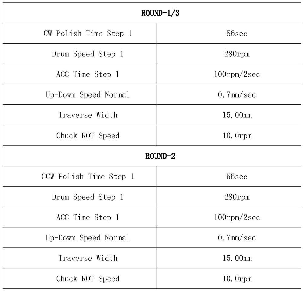
Embodiment 1
[0029] The experimental technique of the present embodiment comprises the following steps:
[0030] S1. First, weigh the 8-inch Czochralski silicon chip, ammonia water, hydrochloric acid, hydrogen peroxide, hydrofluoric acid, and deionized water according to the weight ratio of the components, and place them in corresponding storage containers. Backup internally.
[0031] S2. Then place the 8-inch Czochralski silicon wafer on the BBS edge polishing machine for edge polishing. After the edge polishing is completed, the 8-inch Czochralski silicon wafer, ammonia water, hydrochloric acid, Hydrogen peroxide, hydrofluoric acid, and deionized water are introduced into the cleaning machine to clean the edge-throwing silicon wafers, and an appropriate cleaning solution is added during the cleaning process.
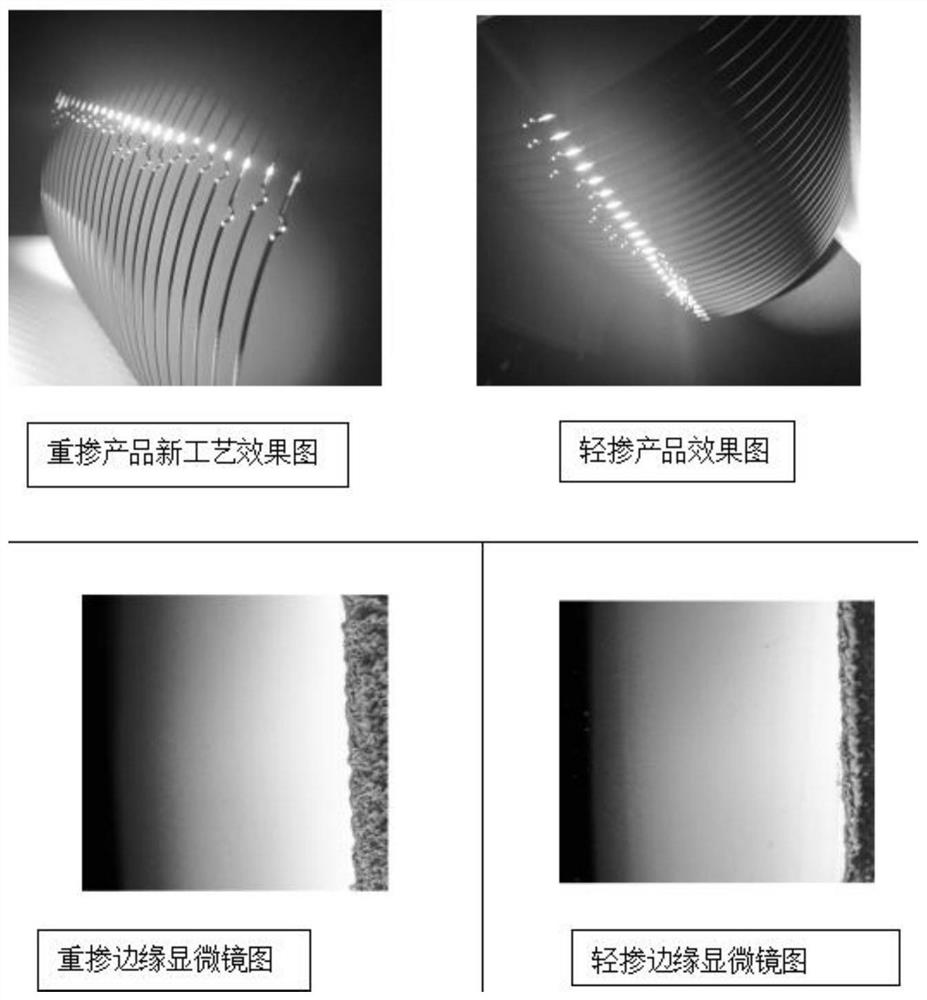
[0032] S3. Finally, the cleaned 8-inch Czochralski silicon wafer can be placed under a strong light, and the edge defects of the silicon wafer can be inspected by real-time observ...
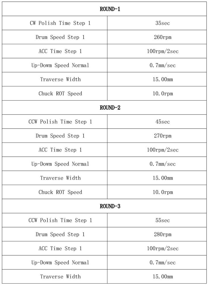
Embodiment 2
[0047] The difference from Embodiment 1 is that:
[0048] The experimental technique of the present embodiment comprises the following steps:
[0049] S1. First, weigh the 8-inch Czochralski silicon chip, ammonia water, hydrochloric acid, hydrogen peroxide, hydrofluoric acid, and deionized water according to the weight ratio of the components, and place them in corresponding storage containers. Backup internally.
[0050]S2. Then place the 8-inch Czochralski silicon wafer on the BBS edge polishing machine for edge polishing. After the edge polishing is completed, the 8-inch Czochralski silicon wafer, ammonia water, hydrochloric acid, Hydrogen peroxide, hydrofluoric acid, and deionized water are introduced into the cleaning machine to clean the edge-throwing silicon wafers, and an appropriate cleaning solution is added during the cleaning process.
[0051] S3. Finally, the cleaned 8-inch Czochralski silicon wafer can be placed under a strong light, and the edge defects of the...
PUM
 Abstract
Description
Claims
Application Information