Unlock instant, AI-driven research and patent intelligence for your innovation.

Pixel unit and manufacturing method thereof, and display device

A technology of pixel unit and pixel area, applied in electrical components, semiconductor/solid-state device manufacturing, electric-solid-state devices, etc., can solve the problem of pixel edge light emission, and achieve the effect of solving pixel edge light emission and difficult climbing effect.

Pending Publication Date: 2021-04-16
BOE TECH GRP CO LTD +1
View PDF0 Cites 0 Cited by
  • Summary
  • Abstract
  • Description
  • Claims
  • Application Information

AI Technical Summary

Problems solved by technology

[0006] In view of this, the object of the present invention is to propose a pixel unit and its manufacturing method and display device to solve the problem of light emitting at the edge of the pixel

Method used


Image

  • Pixel unit and manufacturing method thereof, and display device
  • Pixel unit and manufacturing method thereof, and display device
  • Pixel unit and manufacturing method thereof, and display device

Examples


Embodiment Construction

[0044] In order to make the objectives, technical solutions and advantages of the present invention clearer, the present invention will be further described in detail below with reference to specific embodiments and accompanying drawings.

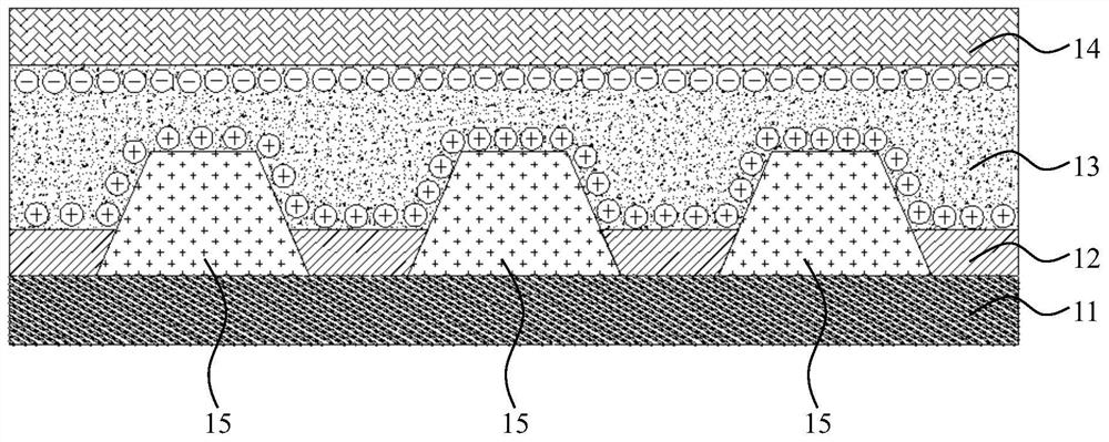
[0045] like figure 2 As shown, it is a schematic structural diagram of a pixel unit according to an embodiment of the present invention, figure 2 A substrate 21 and a pixel unit located on the substrate 21 are shown, the pixel unit includes a pixel defining layer 25, a first electrode 22, an organic layer 23, and a second electrode 24, and the pixel defining layer 25 defines a pixel area, The organic layer 23 is formed in the pixel region and located on the first electrode 22, and the second electrode 24 is formed on the organic layer 23; wherein, the pixel defining layer 25 is provided with at least A groove 26. It can be seen that in the pixel unit provided by the present invention, the organic layer of the adjacent pixel unit is sepa...


PUM

PropertyMeasurementUnit
angleaaaaaaaaaa
angleaaaaaaaaaa

Abstract

The invention discloses a pixel unit and a manufacturing method thereof, and a display device. The pixel unit comprises a substrate, pixel defining layers, a first electrode, organic layers and a second electrode; the pixel defining layers and the first electrode are located on one side of the substrate, and the pixel defining layers define pixel areas; the organic layers are formed in the pixel areas and located on the first electrode; the second electrode is formed on the organic layers; the pixel defining layers comprise at least one groove; at least one bevel edge of each groove comprises a first part away from one side of the substrate and a second part located between the first part and the substrate, and the slope angle of the second part is larger than that of the first part. The grooves are formed in the pixel defining layers to separate the organic layers of the adjacent pixel units, and when the organic layers are evaporated, the organic layers are separated in the grooves and are not easily covered by steps, that is, a climbing effect is not easily generated, and carriers on the first electrode are prevented from moving to a non-pixel area, so that positive charges and electrons are prevented from being compounded in the non-pixel area.

Description

[0001] This application is a divisional application of an invention patent application with an application date of April 20, 2017, an application number of 201710260928.7, and an invention title of "pixel unit and its manufacturing method and display device". technical field [0002] The present invention relates to the field of display technology, in particular to a pixel unit, a manufacturing method thereof, and a display device. Background technique [0003] Organic Lighting-Emitting Diode (OLED) is considered to be a promising alternative to Thin Film Transistor-Liquid Display (TFT) due to its many advantages, such as self-luminescence, thinness, good color gamut, low power consumption and flexibility. Crystal Display, TFT-LCD) is a new generation of display technology. [0004] At present, OLED technology has gradually matured and gradually entered the market, especially small-sized OLED panels. However, due to the large size of the large-size OLED panel, the shadow ef...

Claims


Application Information

Patent Timeline
Patent Type & Authority Applications(China)
IPC IPC(8): H01L27/32H01L51/56
CPCH10K59/121H10K59/122H10K59/12H10K59/10H10K59/1201
Inventor 贾文斌许名宏高昕伟万想朱飞飞
Owner BOE TECH GRP CO LTD
Features
  • R&D
  • Intellectual Property
  • Life Sciences
  • Materials
  • Tech Scout
  • Unparalleled Data Quality
  • Higher Quality Content
  • 60% Fewer Hallucinations
Learn More