Intelligent electroplating device and method for circuit board

A technology for electroplating devices and circuit boards, which is applied in the electrolysis process, electrolysis components, and the formation of electrical connection of printed components, etc., can solve problems such as affecting electroplating efficiency, incapability of intelligent control, and waste of electroplating solution, and achieves convenient operation, accurate electroplating, and improved electroplating. The effect of thickness distribution

Pending Publication Date: 2021-04-20
深圳市合成快捷电子科技有限公司
View PDF20 Cites 0 Cited by
  • Summary
  • Abstract
  • Description
  • Claims
  • Application Information

AI Technical Summary

Problems solved by technology

[0003] When electroplating the through holes on the circuit board, the electroplating is often inaccurate and causes the waste of electroplating solution, and it cannot be intelligently controlled, which affects the electroplating efficiency. Therefore, we propose an intelligent electroplating device and electroplating method for circuit boards. to solve the problems faced by the industry

Method used


Image

  • Intelligent electroplating device and method for circuit board
  • Intelligent electroplating device and method for circuit board
  • Intelligent electroplating device and method for circuit board

Examples


Embodiment Construction

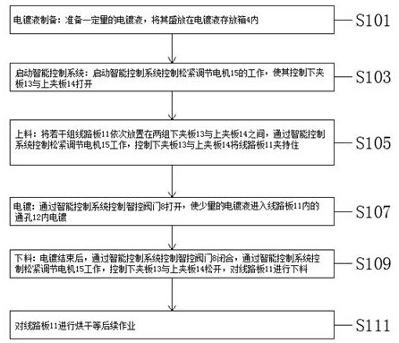
[0027] The following will clearly and completely describe the technical solutions in the embodiments of the present invention with reference to the accompanying drawings in the embodiments of the present invention. Obviously, the described embodiments are only some, not all, embodiments of the present invention. Based on the embodiments of the present invention, all other embodiments obtained by persons of ordinary skill in the art without making creative efforts belong to the protection scope of the present invention.

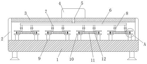
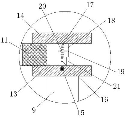
[0028] as attached Figure 1-2 The shown intelligent electroplating device for a circuit board includes a body 1, two support frames 2 are fixedly installed at both ends of the body 1, and an electroplating station 3 is fixedly installed between the upper ends of the two support frames 2, and the electroplating station An electroplating solution storage box 4 is fixedly installed on the top of the electroplating solution storage box 4, and a delivery pipe 5 is...


PUM


Abstract

The invention discloses an intelligent electroplating device and method for a circuit board, and particularly relates to the technical field of circuit board electroplating. The intelligent electroplating device comprises a machine body, two supporting frames are fixedly installed at the two ends of the upper surface of the machine body, an electroplating table is fixedly installed between the upper ends of the two supporting frames, and an electroplating liquid storage box is fixedly installed on the electroplating table. A conveying pipe is installed at the bottom of the electroplating liquid storage box, the conveying pipe penetrates through the electroplating table and extends to one end of the lower side of the electroplating table to be fixedly provided with a liquid uniformizing pipe, a plurality of electroplating pipes are installed below the liquid uniformizing pipe, and a plurality of sets of supporting seat rods are fixedly installed on the machine body. When through holes in the circuit board are electroplated, operation is convenient and fast, electroplating is accurate, electroplating efficiency is improved, meanwhile, waste of electroplating liquid can be reduced, the electroplating liquid used in the method is beneficial for improving hole filling quality, scratches and other microcosmic distribution of the circuit board, and meanwhile macroscopic coating thickness distribution is also better improved.

Description

technical field [0001] The invention relates to the technical field of circuit board electroplating, and more specifically, the invention relates to an intelligent electroplating device and an electroplating method for circuit boards. Background technique [0002] Circuit boards include: ceramic circuit boards, alumina ceramic circuit boards, aluminum nitride ceramic circuit boards, circuit boards, PCB boards, aluminum substrates, high-frequency boards, thick copper boards, impedance boards, PCB, ultra-thin circuit boards, ultra-thin circuits boards, printed (copper etching technology) circuit boards, etc. The circuit board makes the circuit miniaturized and intuitive, and plays an important role in mass production of fixed circuits and optimizing the layout of electrical appliances. The circuit board can be called a printed circuit board or a printed circuit board, and the FPC circuit board (FPC circuit board is also called a flexible circuit board). , an excellent flexib...

Claims


Application Information

Patent Timeline
Patent Type & Authority Applications(China)
IPC IPC(8): C25D17/00C25D17/08C25D5/02C25D7/00C25D3/38H05K3/42
Inventor 雷成
Owner 深圳市合成快捷电子科技有限公司
Why Eureka
Try Eureka